Transistor, resistance variable memory device including the same, and manufacturing method thereof

a technology of resistance variable and transistor, which is applied in the direction of digital storage, semiconductor devices, instruments, etc., can solve the problems of gate induced drain leakage (girl), the study of existing electronic charge controlled devices is expected to encounter the limitation, and the gate induced drain leakage may be caused

Inactive Publication Date: 2014-08-28
SK HYNIX INC
View PDF4 Cites 32 Cited by
  • Summary
  • Abstract
  • Description
  • Claims
  • Application Information

AI Technical Summary

Benefits of technology

[0013]According to still another aspect of an exemplary embodiment of the present invention, a method of manufacturing a resistance variable semiconductor device may include forming a source region in a semiconductor substrate, forming a semiconductor layer on the source region, patterning the semiconductor layer to form an active pillar, forming a first gate electrode to surround the active pillar, surrounding an upper region of the first gate electrode with an insulating layer while exposing a lower region of the first gate electrode, and forming a second gate electrode by increasing a work function of the exposed first gate electrode.

Problems solved by technology

With the rapid development of mobile and digital information communication and consumer-electronic industry, studies on existing electronic charge controlled-devices are expected to encounter the limitation.
However, even in the 3D vertical transistors, thin gate insulating layers may be required.
Thus, when a high voltage is supplied to a gate, a high electric field is applied to a lightly doped drain (LDD) region and gate induced drain leakage (GIRL) may be caused.

Method used


Image

  • Transistor, resistance variable memory device including the same, and manufacturing method thereof
  • Transistor, resistance variable memory device including the same, and manufacturing method thereof
  • Transistor, resistance variable memory device including the same, and manufacturing method thereof

Examples


Embodiment Construction

”.

BRIEF DESCRIPTION OF THE DRAWINGS

[0015]The above and other aspects, features and other advantages of the subject matter of the present disclosure will be more clearly understood from the following detailed description taken in conjunction with the accompanying drawings, in which:

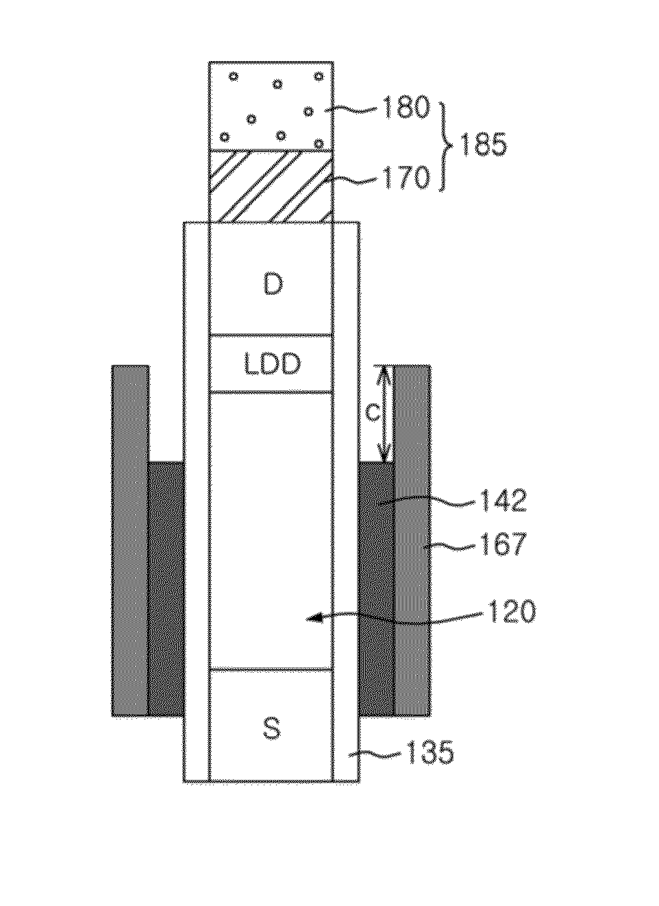
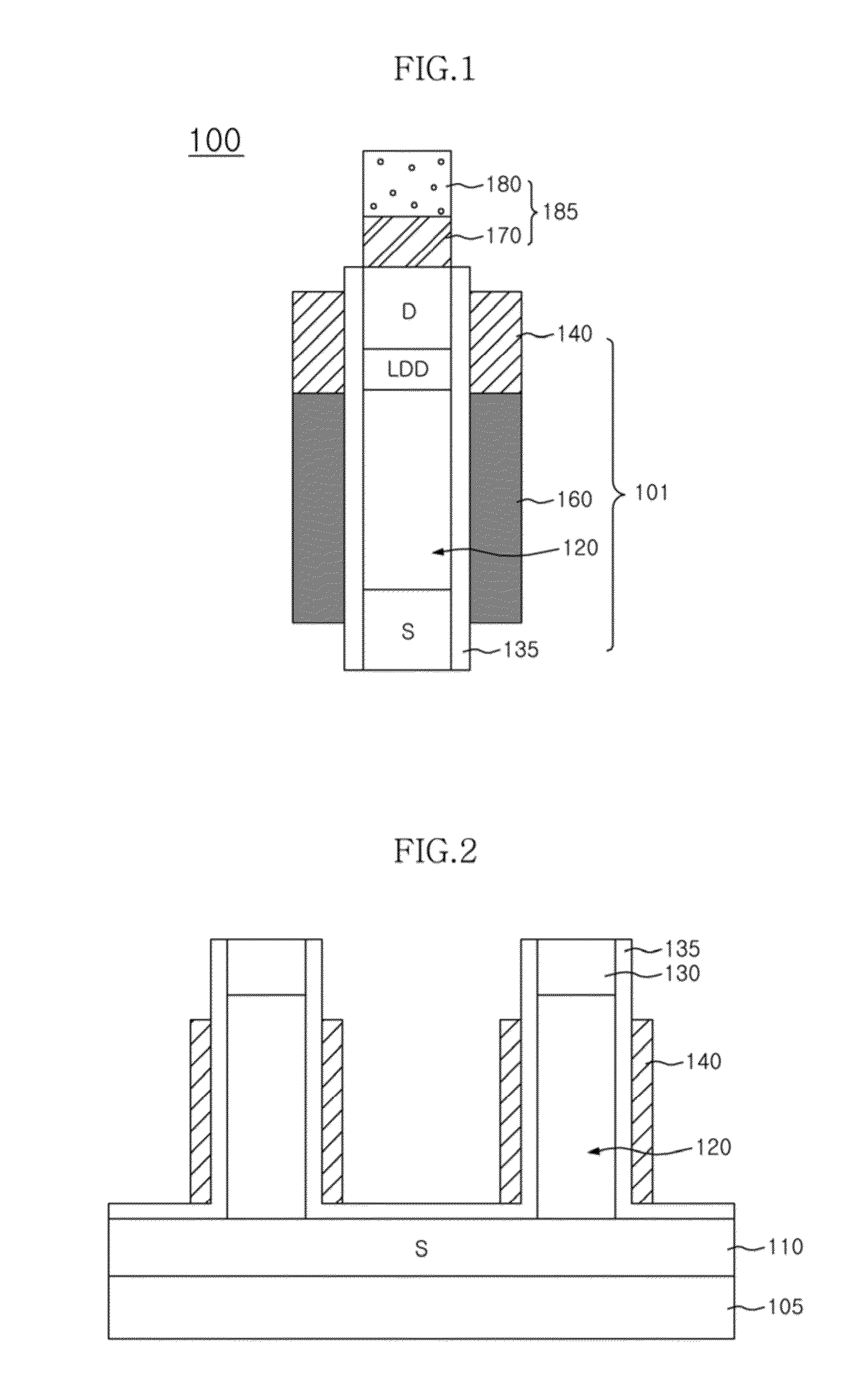
[0016]FIG. 1 is a schematic cross-sectional view illustrating a resistance variable memory device including a vertical transistor according to an exemplary implementation of the inventive concept;

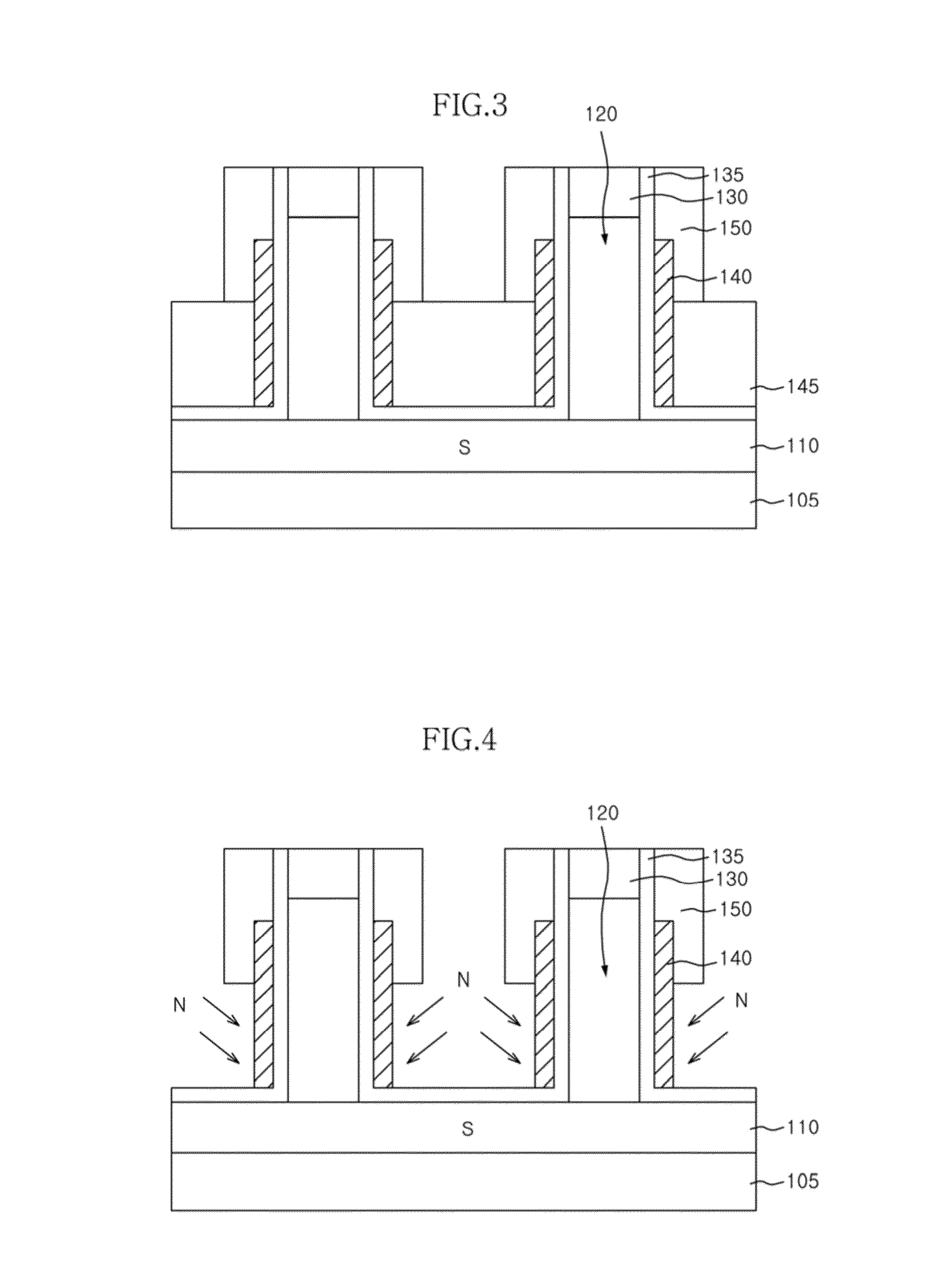
[0017]FIGS. 2 to 5 are cross-sectional views sequentially illustrating a process of manufacturing a vertical transistor of a resistance variable memory device according to an exemplary implementation of the inventive concept;

[0018]FIG. 6 is a schematic cross-sectional view illustrating a resistance variable memory device including a vertical transistor according to another exemplary implementation of the inventive concept;

[0019]FIGS. 7 and 8 are cross-sectional views sequentially illustrating a process of manufact...


PUM


Abstract

A resistance variable memory device including a vertical transistor includes an active pillar including a channel region, a source formed in one end of the channel region, and a lightly doped drain (LDD) region and a drain formed in the other end of the channel region, a first gate electrode formed to surround a periphery of the LDD region and having a first work function, and a second gate electrode formed to be connected to the first gate electrode and to surround the channel region and having a second work function that is higher than the first to work function.

Description

CROSS-REFERENCES TO RELATED APPLICATION[0001]The present application claims priority under 35 U.S.C, 119(a) to Korean application number 10-2013-0021164, filed on Feb. 27, 2013, in the Korean Intellectual Property Office, which is incorporated herein by reference in its entirety.BACKGROUND[0002]1. Technical Field[0003]Exemplary embodiments of the present invention relate to a semiconductor integrated circuit device, and more particularly, to a transistor, and a resistance variable memory device including the same, and a manufacturing method thereof.[0004]2. Related Art[0005]With the rapid development of mobile and digital information communication and consumer-electronic industry, studies on existing electronic charge controlled-devices are expected to encounter the limitation. Thus, new functional memory devices of new concept other than the existing electronic charge devices need to be developed. In particular, next-generation memory devices with large capacity, ultra-high speed, ...

Claims


Application Information

Patent Timeline
Patent Type & Authority Applications(United States)
IPC IPC(8): H01L27/24H01L21/8234H01L29/78
CPCH01L27/2454H01L21/8234H01L29/7827H01L29/7833H01L21/823487H01L27/101H01L29/66666H10B63/34H10B61/22H10B63/80H10N50/80H10N50/10H10N70/24H10N50/01H10N70/231H10N70/882H10N70/8845H10N70/826H10N70/021H01L29/78H01L29/42376H01L29/4236H01L29/4975H01L29/4983G11C13/0002H01L29/4966H01L29/66484H10N52/00H10N70/841H01L29/45H01L29/495H01L29/7835H01L29/42356H01L29/7834H01L29/42372
Inventor PARK, NAM KYUN
Owner SK HYNIX INC
Why Eureka
Try Eureka