Graphene plasmonic communication link

a graphene plasmonic and communication link technology, applied in the field of communication links, can solve the problems of weak damping of ac current in metal wires, limiting the use of communication methods relying on electrical transport, and deteriorating the overall performance of the communication between the different signals

Inactive Publication Date: 2014-09-11
IBM CORP
View PDF11 Cites 1 Cited by
  • Summary
  • Abstract
  • Description
  • Claims
  • Application Information

AI Technical Summary

Benefits of technology

[0008]A signal transfer link includes a first plasmonic coupler, a second plasmonic coupler disposed in a same plane as the first plasmonic coupler and spaced apart from the first plasmonic coupler by a gap and an insulator layer formed over end portions of the first and second plasmonic couplers and in and over the gap. The insulator has a thickness configured to prevent electrical connection between the first and second plasmonic couplers. A plasmonic conductive layer includes graphene formed over the gap on the insulator layer and overlaps the end portions of the first and second plasmonic couplers such that an electrical signal from one of the first and second plasmonic couplers is converted to a plasmonic signal in the plasmonic conductive layer, which is then converted back to an electrical signal in the other of the first and second plasmonic couplers.
[0009]A method for high frequency signal transfer includes providing a plasmonic signal transfer link including a first plasmonic coupler, a second plasmonic coupler spaced apart from the first plasmonic coupler to form a gap, an insulator layer formed over end portions of the first and second plasmonic couplers and in and over the gap, and a plasmonic conductive layer formed over the gap on the insulator layer to excite plasmons to provide signal transmission between the first and second plasmonic couplers; and signaling between a first component coupled to the first plasmonic coupler and a second component coupled to the second plasmonic coupler at a frequency between about 100 GHz and 10 THz.

Problems solved by technology

For signal frequencies above a few 100 GHz, the AC current in a metal wire is subject to strong damping, and losses associated with signal progression limit the use of communication methods that rely on electrical transport.
For multiple closely spaced transmitter-receiver systems, however, the interference (cross-talk) between the different signals deteriorates the overall performance and limits practical applications.

Method used


Image

  • Graphene plasmonic communication link
  • Graphene plasmonic communication link
  • Graphene plasmonic communication link

Examples


Embodiment Construction

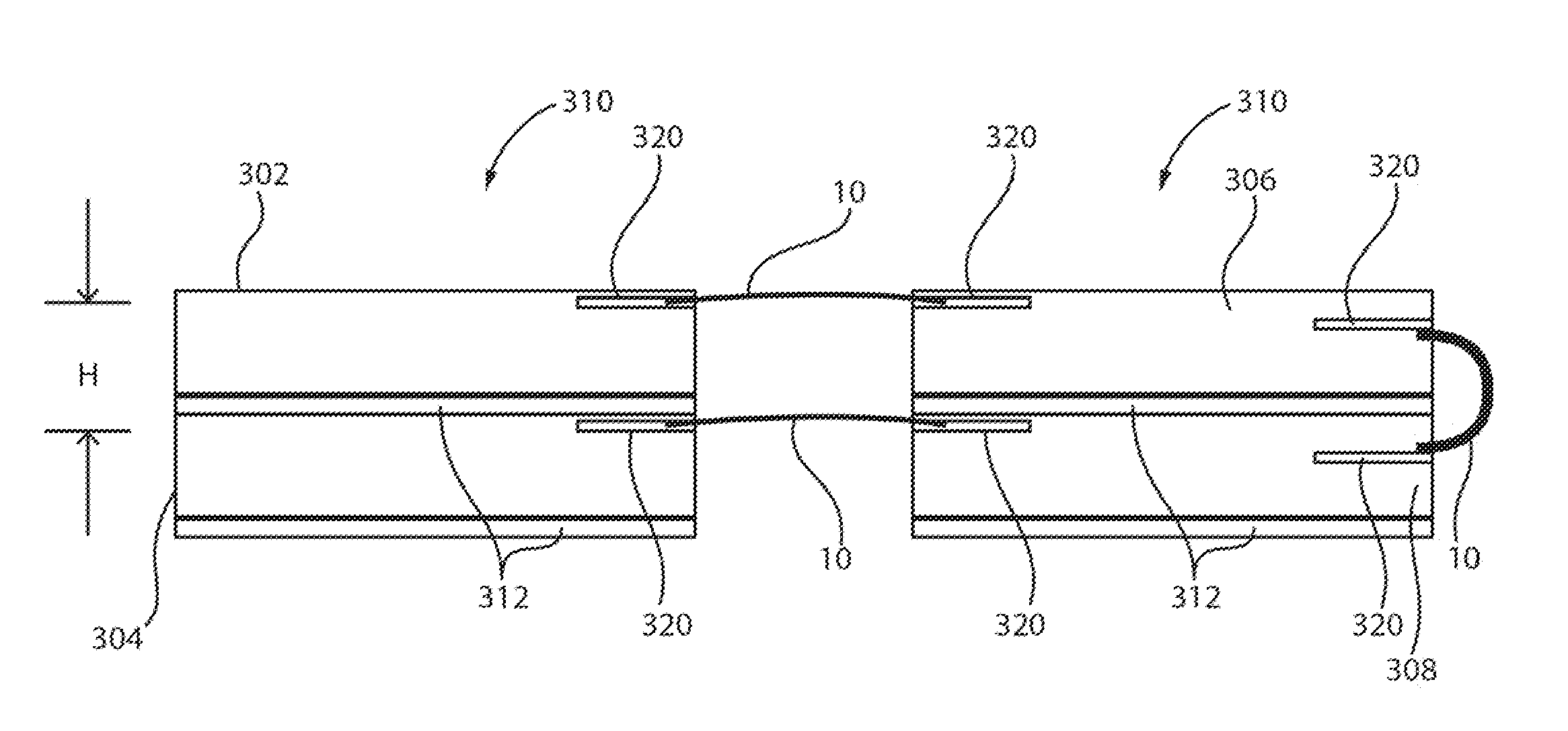
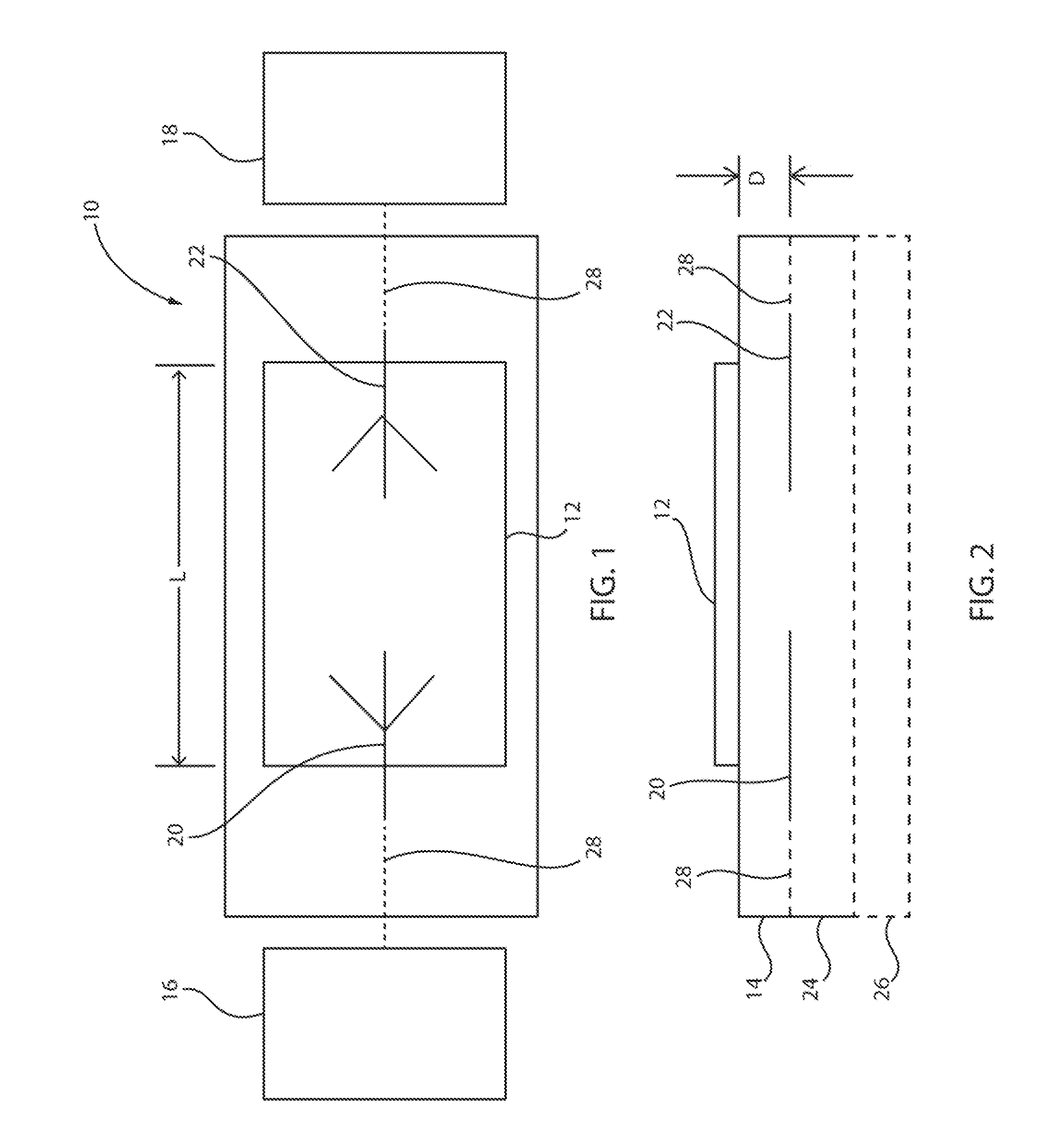
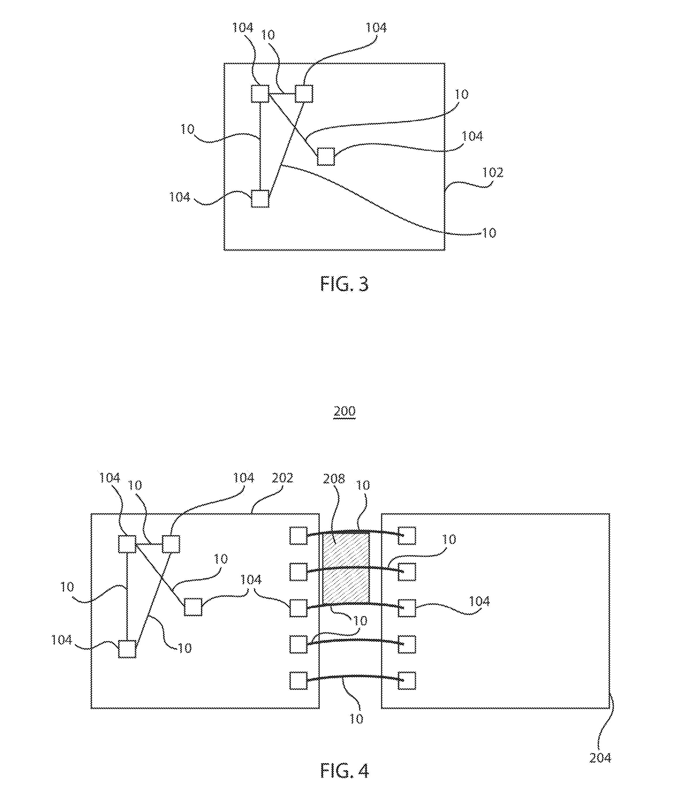
[0020]In accordance with the present principles, a plasmon-based communication link is provided that overcomes the limitations of the prior art. The plasmon-based communication link includes a non-radiative, plasmon-mediated signal transport mechanism that neither relies on electrical transport nor on far-field radiation electromagnetic waves. The plasmon-mediated communication channel permits signal transmission at Terahertz frequencies. The plasmon -based communication link as described herein is particularly useful in intra-chip and inter-chip communications, although the present principles are applicable to any communication link or system.

[0021]In one example, a layer (or few layers) of graphene form a mono-atomic carbon layer, for plasmon-mediated inter-systems communications. Plasmons are collective excitations of charge carriers in graphene, and are excited at one end of the graphene-based plasmonic link by a plasmon launcher (e.g., a plasmon coupler or plasmon antenna) atta...


PUM


Abstract

A signal transfer link includes a first plasmonic coupler, and a second plasmonic coupler spaced apart from the first plasmonic coupler to form a gap. An insulator layer is formed over end portions of the first and second plasmonic couplers and in and over the gap. A plasmonic conductive layer is formed over the gap on the insulator layer to excite plasmons to provide signal transmission between the first and second plasmonic couplers.

Description

RELATED APPLICATION DATA[0001]This application is a Continuation application of co-pending U.S. patent application Ser. No. 13 / 790,830 filed on Mar. 8, 2013, incorporated herein by reference in its entirety.BACKGROUND[0002]1. Technical Field[0003]The present invention relates to communication links, and more particularly to inter- and intra-integrated circuit chip communication using graphene plasmonic communication links.[0004]2. Description of the Related Art[0005]Electromagnetic communication between components of a system at high frequencies is a fundamental requirement for the advancement of high-performance computing and the information technology (IT) industry. The higher the carrier frequency of an electrical signal, the more bandwidth is available, which translates into a larger amount of information that can be transferred.[0006]Current commercial communication systems operate at frequencies below 80 GHz. For signal frequencies above a few 100 GHz, the AC current in a meta...

Claims


Application Information

Patent Timeline
Patent Type & Authority Applications(United States)
IPC IPC(8): H04B10/80
CPCH04B10/801G02B6/1226H04B10/90B82Y20/00G02B6/262G02B2006/12142G02B2006/12147G02F2203/10G02F2203/13G02F2203/50H04B10/802
Inventor AVOURIS, PHAEDONPAREBEINOS, VASILISTEINER, MATHIAS B.VALDES GARCIA, ALBERTO
Owner IBM CORP
Why Eureka
Try Eureka