Dsa grapho-epitaxy process with etch stop material

a grapho-epitaxy and stop material technology, applied in the field of semiconductor/solid-state device manufacturing, basic electric elements, electric devices, etc., can solve the problems of high defect level, large resist feature size, and inability to form high-resolution mandrels, so as to reduce the width of the template structure

Inactive Publication Date: 2014-09-11
IBM CORP
View PDF19 Cites 166 Cited by
  • Summary
  • Abstract
  • Description
  • Claims
  • Application Information

AI Technical Summary

Benefits of technology

[0009]A method for patterning electronic structures using directed self-assembly (DSA) materials includes forming an etch stop layer on a neutral material over a substrate; forming a tri-layer lithographic mask pattern layer on the etch stop layer including an optical planarization layer (OPL), an anti-reflection coating (ARC) on the OPL and a resist layer on the ARC; developing the resist layer using optical lithography to form a template pattern on the ARC; reactive ion etching the ARC and the OPL down to the etch stop layer in accordance with the template pattern to form a template structure; removing the ARC from the OPL and trimming the template structure to reduce a width of the

Problems solved by technology

However, present techniques yield large inaccurate resist features, which cannot form high resolution mandrels.
Further, metal lift-off processes from resist features require metal deposition onto a neutral material layer leading to high defect levels and high line edge roughness (LER).
Employing e-beam resists to form resist patterns on top of the neutral materia

Method used


Image

  • Dsa grapho-epitaxy process with etch stop material
  • Dsa grapho-epitaxy process with etch stop material
  • Dsa grapho-epitaxy process with etch stop material

Examples


Embodiment Construction

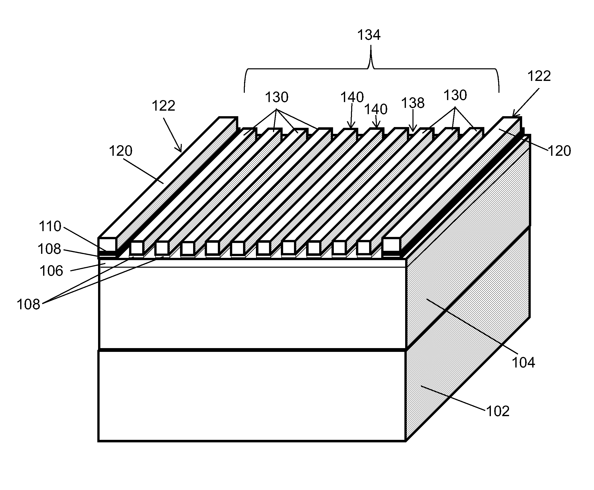
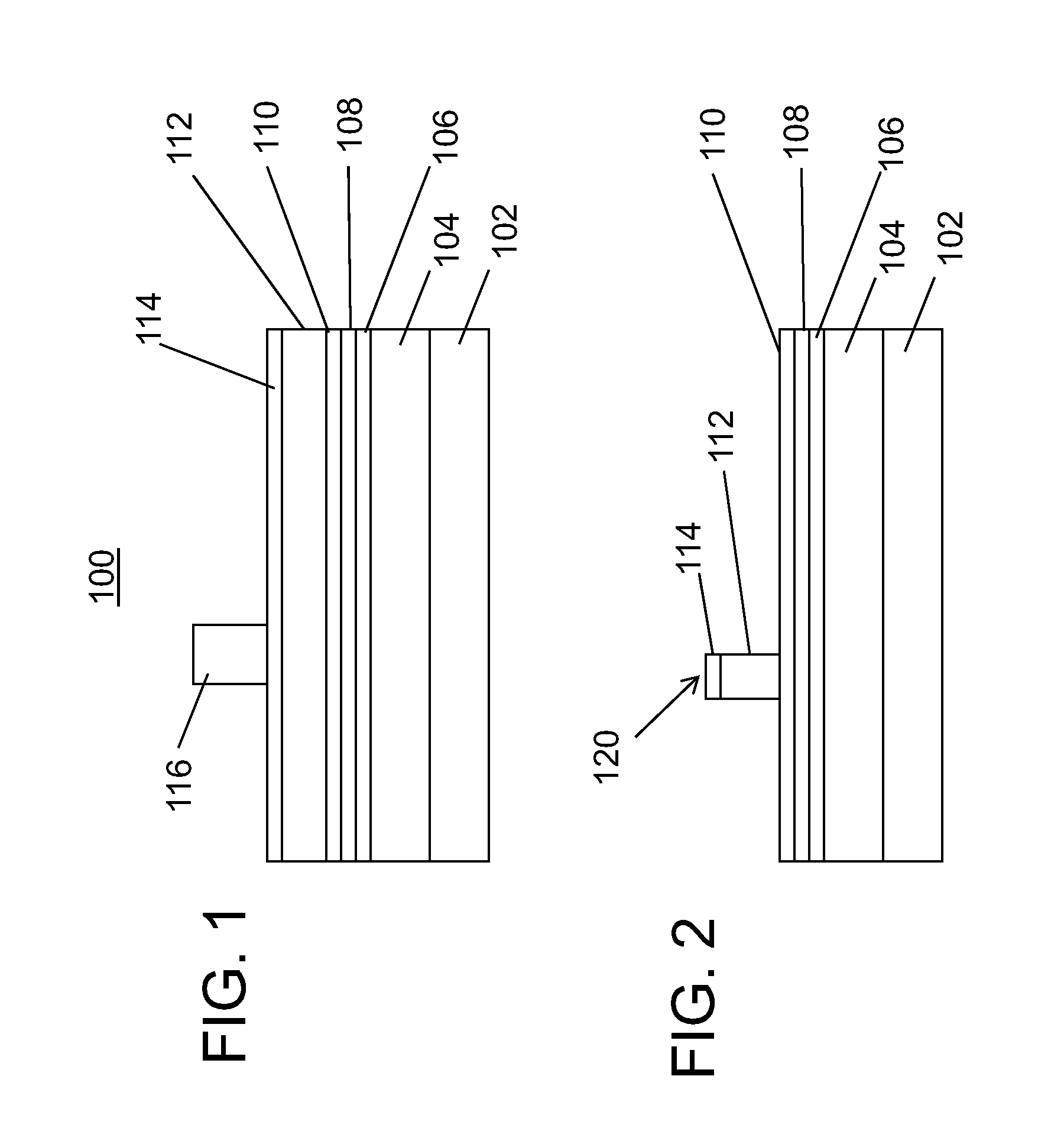
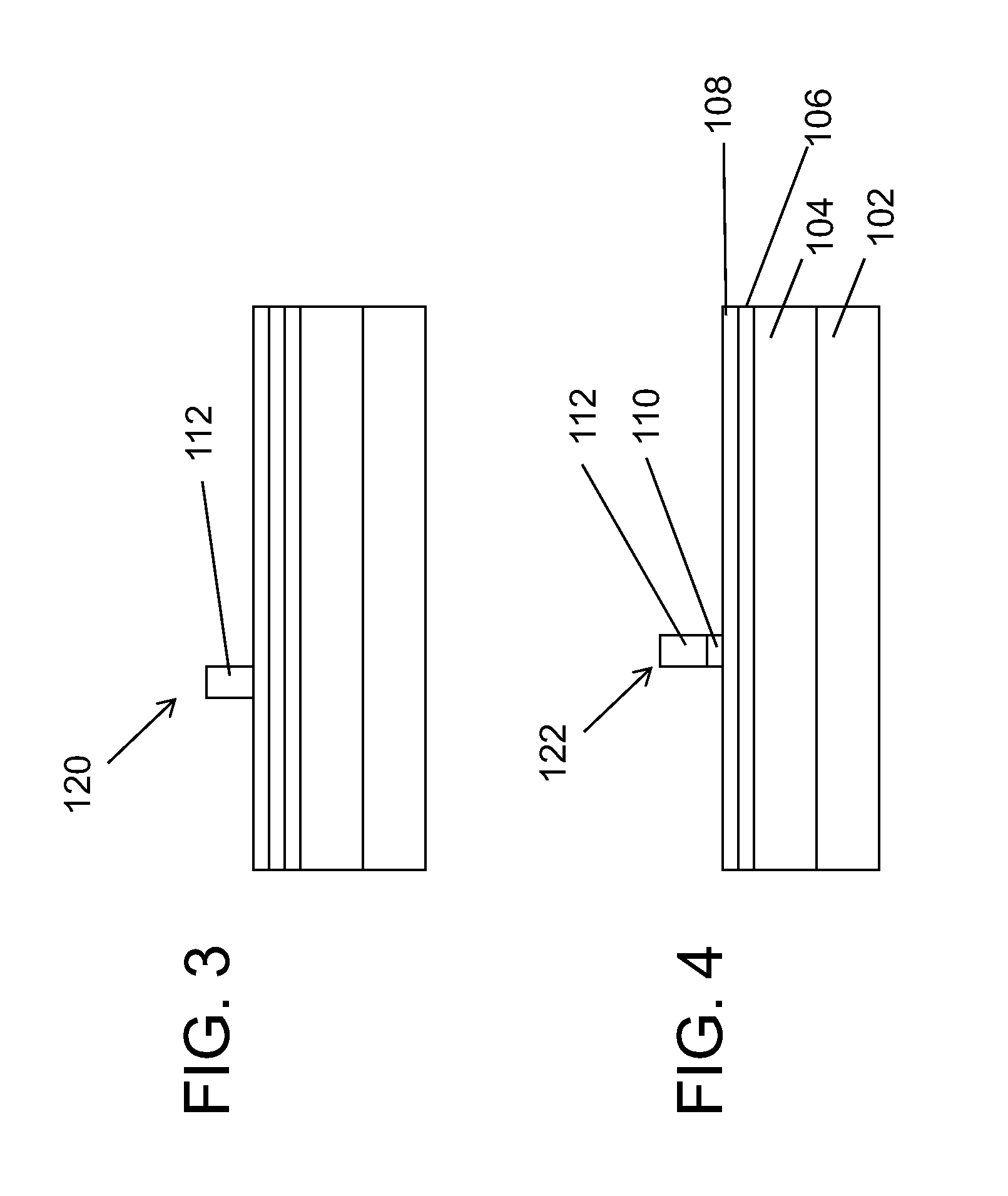
[0020]In accordance with the present principles, devices and methods are described for providing high-resolution templates for directed self-assembly (DSA) structures. While the present embodiments will be described with respect to templates for DSA, it should be understood that the present principles may be applied to any semiconductor fabrication process. In one embodiment, a multi-layer structure employs lithography and etch stop / release layers to provide the high-resolution template. In a particularly useful embodiment, a resist layer, anti-reflection coating (ARC), an optical planarization layer (OPL) and etch stop layer are employed together to form a stack structure. The resist is lithographically patterned and employed as an etch mask to etch narrow lines (e.g., 10-20 nm) in the ARC, OPL and, eventually, the etch stop layer. The etch stop layer functions as a combined etch stop and release layer under the stack for ease of removal of patterning film without damaging a neutra...


PUM


Abstract

A method for defining a template for directed self-assembly (DSA) materials includes forming an etch stop layer on a neutral material, forming a mask layer on the etch stop layer and forming an anti-reflection coating (ARC) on the mask layer. A resist layer is patterned on the ARC using optical lithography to form a template pattern. The ARC and the mask layer are reactive ion etched down to the etch stop layer in accordance with the template pattern to form a template structure. The ARC is removed from the mask layer and the template structure is trimmed to reduce a width of the template structure. A wet etch is performed to remove the etch stop layer to permit the neutral material to form an undamaged DSA template for DSA materials.

Description

BACKGROUND[0001]1. Technical Field[0002]The present invention relates to semiconductor processing, and more particularly to methods for achieving high resolution resist structures for template formation for directed self-assembly (DSA) processing.[0003]2. Description of the Related Art[0004]Directed self assembly (DSA) has emerged as a useful tool in semiconductor processing. DSA includes providing two materials and polymerizing them to concurrently form the materials into separate polymer regions. By providing physical guides, mandrels or templates, the polymers can be formed into useful structures, e.g., parallel lines and the like. DSA may be employed, e.g., to form interconnect lines, spacers and / or contacts.[0005]DSA typically requires high-resolution templates to ensure proper formation of the DSA structures. However, present techniques yield large inaccurate resist features, which cannot form high resolution mandrels. Further, metal lift-off processes from resist features req...

Claims


Application Information

Patent Timeline
IPC IPC(8): H01L21/308
CPCH01L21/308H01L21/0337H01L21/0271
Inventor ABDALLAH, JASSEM A.COLBURN, MATTHEW E.HOLMES, STEVEN J.KAWAMURA, DAIJILIU, CHI-CHUNSANKARAPANDIAN, MUTHUMANICKAMYIN, YUNPENG
Owner IBM CORP
Why Eureka
Try Eureka