Touch panel structural and display device using touch panel

a technology of touch panel and structure, applied in the field of display devices, can solve the problems of lower resolution, accuracy, long manufacturing time, and long manufacturing time, and achieve the effects of improving the structure of the untouch area of the touch panel, facilitating the circuit design of the conductive circuit layer and yield rate, and saving manufacturing costs

Inactive Publication Date: 2014-09-18
TECO NANOTECH CO LTD
View PDF4 Cites 3 Cited by
  • Summary
  • Abstract
  • Description
  • Claims
  • Application Information

AI Technical Summary

Benefits of technology

[0007]The main object of the present invention is to solve the disadvantages of related arts and thus provide a touch panel structure, which is to improve an un-touch area structure of the touch panel, so that a conductive circuit layer is directly distributed on the un-touch area, the conductive circuits on the conductive circuit layer may not be affected by defect conduction caused by barrier blocks (conductive layer) of the un-touch area in order to facilitate the circuit design of the conductive circuit layer and yield rate, and save cost to manufacturing as well.

Problems solved by technology

Further, ITO layer may happen resistor uneven distribution phenomenon so as to cause problems of lower resolution, accuracy, etc.
The transparent conductive layer of Carbon nano tubes shall use conductive circuits and control circuits to transmit capacitance signals, and hence using Carbon nano tubes may cause the problems of processes and structure.
Such manufacturing may cause longer manufacturing time and more complicate procedures.

Method used


Image

  • Touch panel structural and display device using touch panel
  • Touch panel structural and display device using touch panel
  • Touch panel structural and display device using touch panel

Examples


Embodiment Construction

[0044]Following preferred embodiments and figures will be described in detail so as to achieve aforesaid objects.

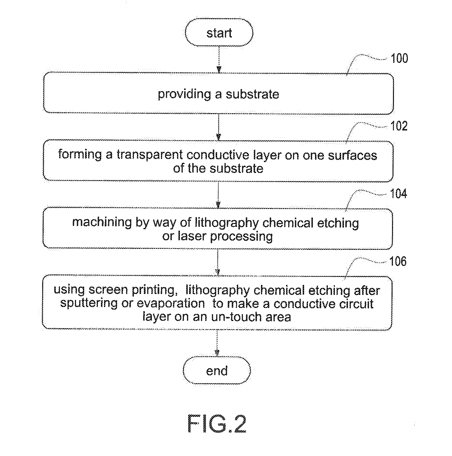
[0045]With references to FIG. 2 to FIG. 6, which illustrate a manufacturing flow chart of the touch panel of the present invention and schematic views of manufacturing steps of the touch panel of the present invention. As shown in figures, the method includes the steps of:

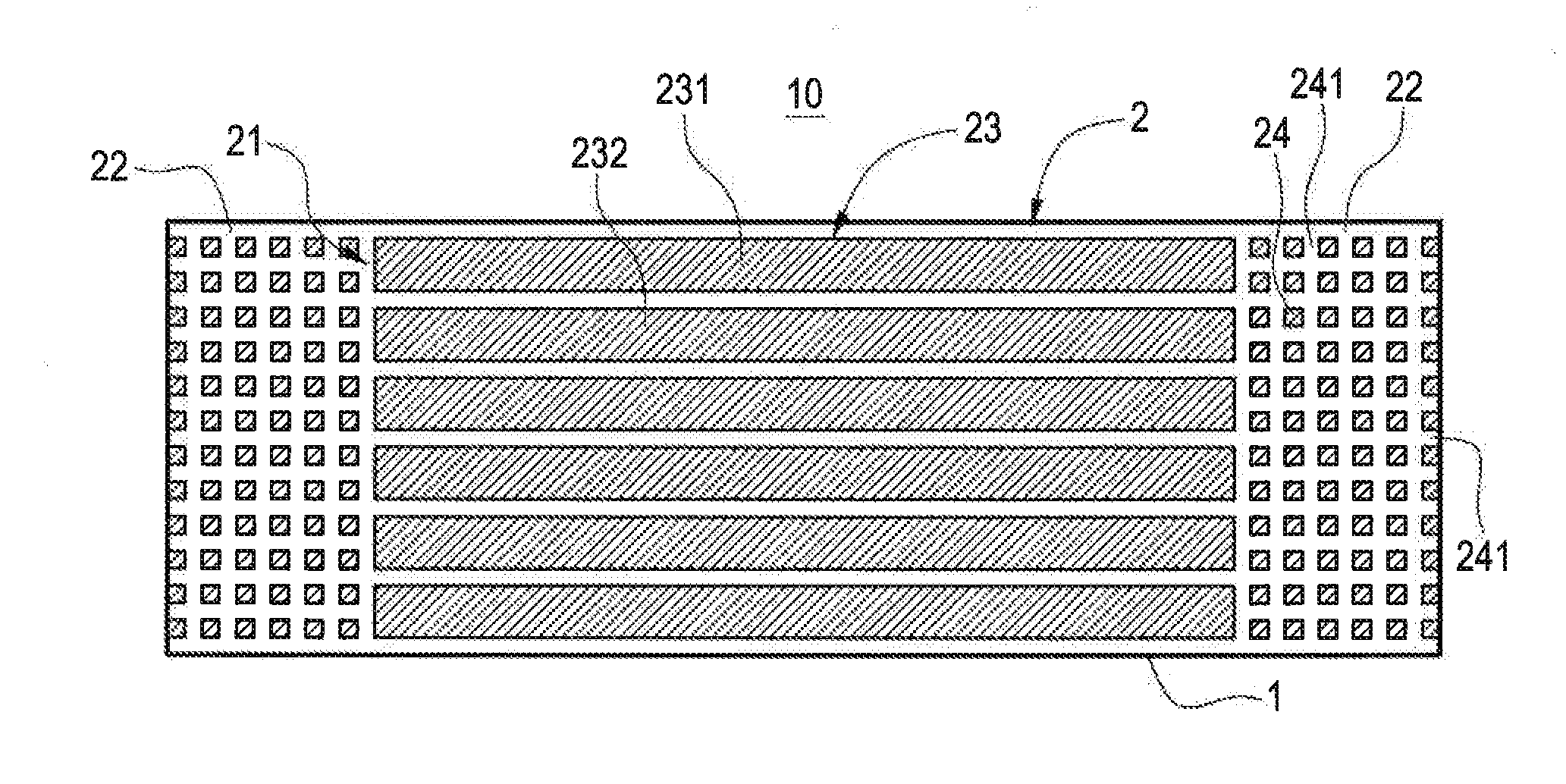
[0046](100) providing a substrate 1, which is made of transparent plastic or transparent glass;

[0047](102) forming a transparent conductive layer 2 on one or two surfaces of the substrate 1, the transparent conductive layer 2 having a touch area 21 and an un-touch area 22, wherein the transparent conductive layer 2 is indium tin oxide (ITO) and oriented carbon nano tube (CNT) in order to let the transparent conductive layer 2 have uniform distribution of electric resistance, further that taking CNT as the transparent conductive layer 2 may let the transparent conductive layer 2 be with a better character...


PUM


Abstract

A touch panel comprises: a substrate, a transparent conductive layer and a conductive circuit layer. The transparent conductive layer is formed on a surface of the substrate, and the transparent conductive layer has a touch area and an un-touch area. The un-touch area has a plurality of barrier blocks arranged in a matrix, and the barrier blocks form a plurality of vertical and horizontal barrier slots. The conductive circuit layer is directly distributed on the barrier slots formed by the barrier blocks of the touch area, so as to increase the space to distributing circuits on the conductive circuit layer and save cost to manufacturing.

Description

BACKGROUND OF THE INVENTION[0001]1. Field of the Invention[0002]The present invention generally relates to a display device, more particularly to a display device that has a transparent touch panel.[0003]2. Description of the Related Art[0004]Accompany with mobile communication devices as mobile phone, navigation system, etc., which performances and versatileness are highly developed, electronic devices equipped with transparent touch panels in front of display devices are increasing. Based on the work principles and transmission media of touch panels, the current touch panels are four kinds of resistive, capacitive, infrared and surface acoustic wave, wherein the capacitive touch panel is broadly applied since its high accuracy, strong anti-jamming capability.[0005]For the structure of a touch panel, a transparent conductive layer is an important factor. Generally speaking, the transparent conductive layer is always an ITO layer, but ITO layer as transparent conductive layer may ha...

Claims


Application Information

Patent Timeline
Patent Type & Authority Applications(United States)
IPC IPC(8): G06F3/041
CPCG06F3/041G06F2203/04103G06F3/04164
Inventor CHAN, TE-FONGDING, DING-KUOKAO, CHENG-CHIEHCHANG, YU-YANGCHEN, YAO-ZONG
Owner TECO NANOTECH CO LTD
Why Eureka
Try Eureka