Interference filter, interference filter manufacturing method, optical module, electronic apparatus, and bonded substrate

Inactive Publication Date: 2014-09-18
SEIKO EPSON CORP
View PDF9 Cites 13 Cited by
  • Summary
  • Abstract
  • Description
  • Claims
  • Application Information

AI Technical Summary

Benefits of technology

[0070]In this bonded substrate, a pair of substrates are bonded to each other to seal the internal space between these substrates in an airtight manner. In this case, in the bonding portion, the base layer is provided on one of the pair of substrates, the first metal layer is provided so as to cover the base layer, and the first metal layer and the second metal layer provided on the other substrate are bonded to each other. In such

Problems solved by technology

In particular, when processing a substrate by etching or the like, there is a problem in that it is difficult to maintain the surface accuracy.
In addition, when bonding substrates to each other using, for example, a resin layer, adhesive, or low-melting-point glass, it is not possible to sufficiently ensure the airtightness.
For this reason, there is a problem of outgassing and the like.
Accordingly, even if the surface accuracy of the surface of each metal layer is poor at the time of metal bonding between the first and second metal layers, the unevenness of the surface is absorbed since b

Method used


Image

  • Interference filter, interference filter manufacturing method, optical module, electronic apparatus, and bonded substrate
  • Interference filter, interference filter manufacturing method, optical module, electronic apparatus, and bonded substrate
  • Interference filter, interference filter manufacturing method, optical module, electronic apparatus, and bonded substrate

Examples


Example

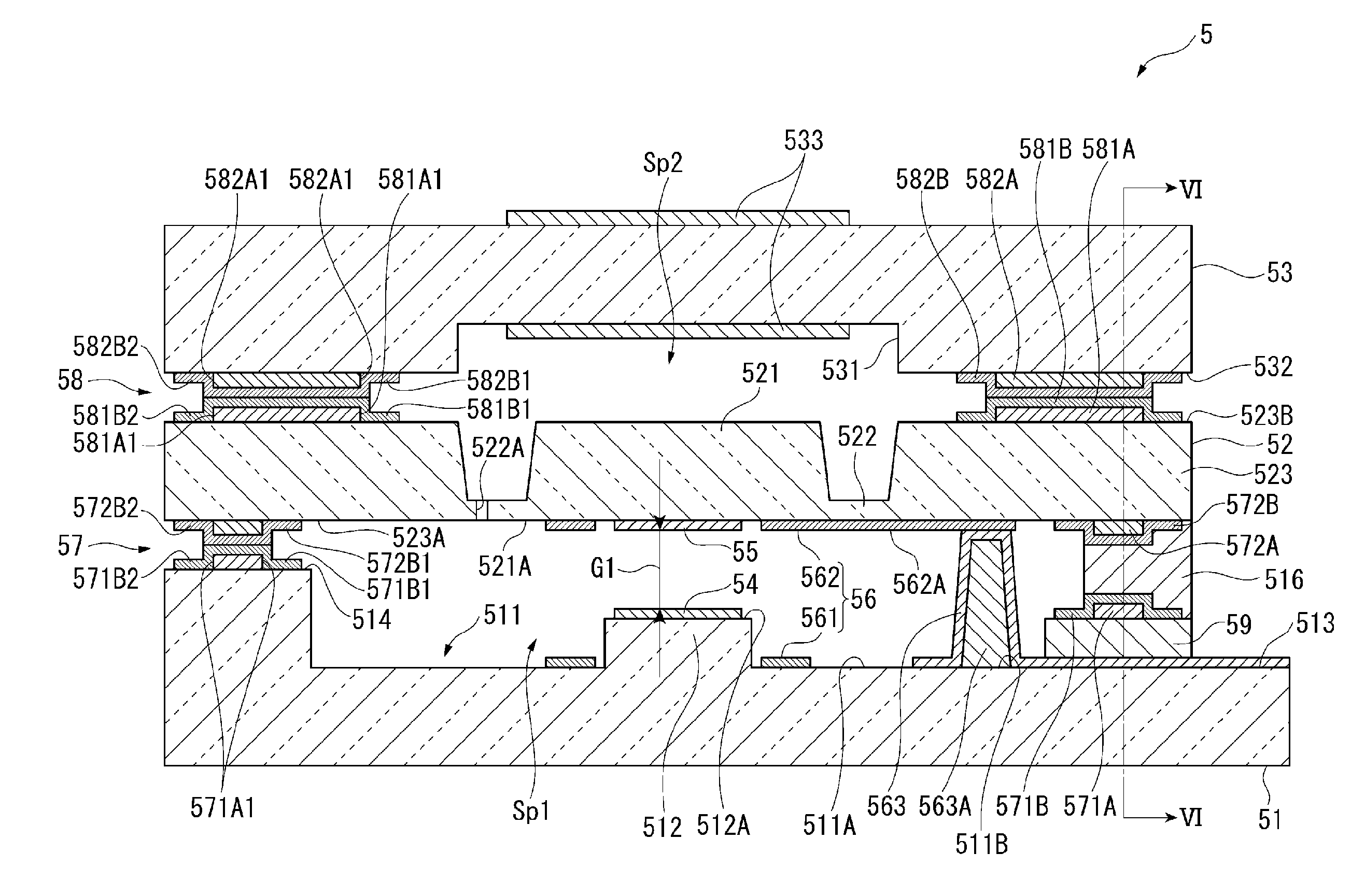
[0091]Hereinafter, a first embodiment of the invention will be described with reference to the accompanying diagrams.

Configuration of a Spectrometer

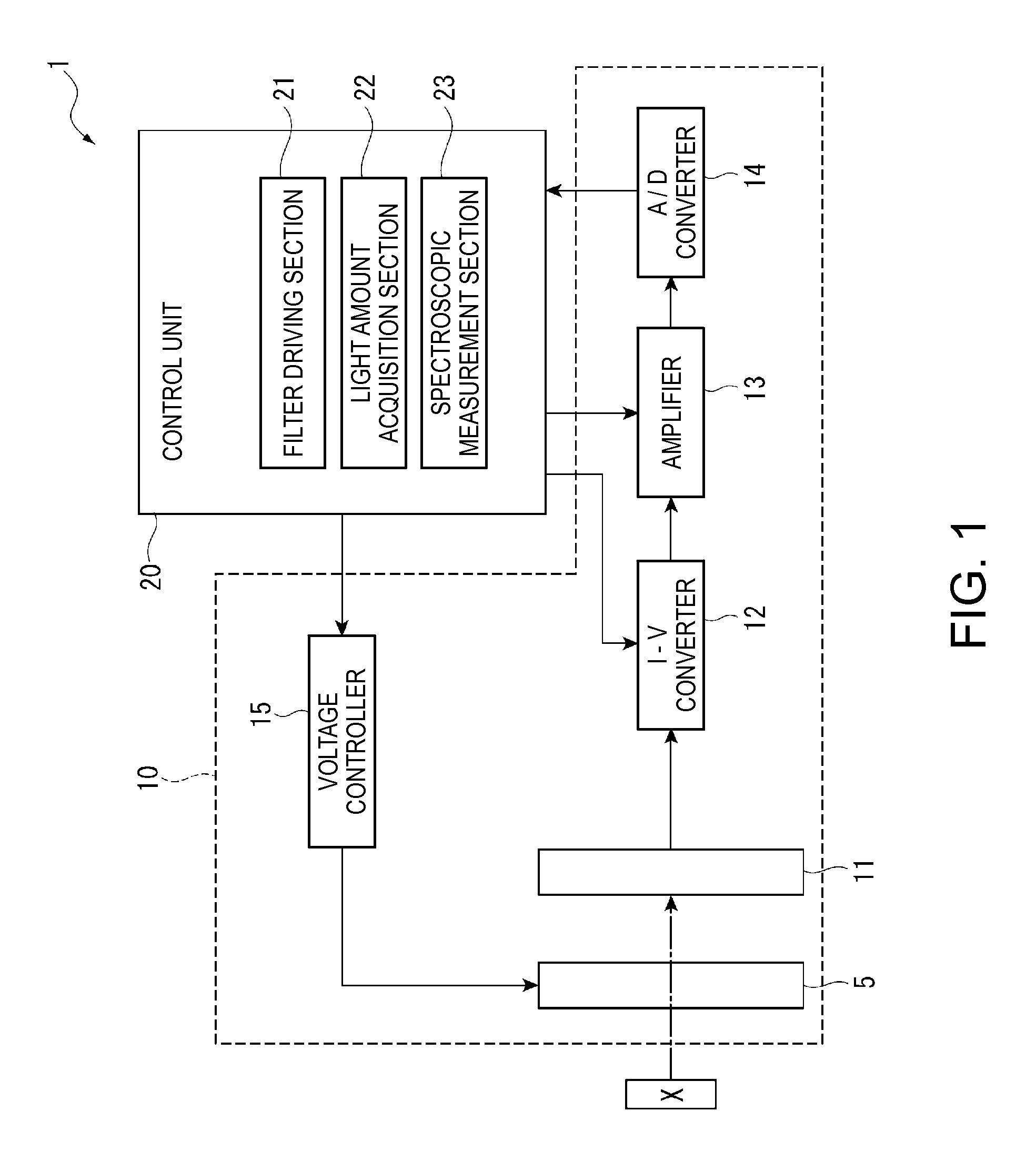
[0092]FIG. 1 is a block diagram showing the schematic configuration of a spectrometer according to the first embodiment of the invention.

[0093]A spectrometer 1 is an example of an electronic apparatus according to the invention, and is an apparatus that analyzes the light intensity of each wavelength in measurement target light reflected by a measurement target X and measures the spectrum. In the present embodiment, an example is shown in which the measurement target light reflected by the measurement target X is measured. However, for example, when a light emitter such as a liquid crystal panel is used as the measurement target X, light emitted from the light emitter may be used as the measurement target light.

[0094]As shown in FIG. 1, the spectrometer 1 includes an optical module 10 and a control unit 20 that processes a signal output ...

Example

Second Embodiment

[0229]Next, a second embodiment of the invention will be described with reference to the accompanying diagrams.

[0230]In the first embodiment described above, the example has been illustrated in which the bonding target surfaces 514, 523A, 523B, and 532 are planes and the resin layers 571A, 572A, 581A, and 582A, which are base layers, are formed on the bonding target surfaces 514, 523A, 523B, and 532.

[0231]However, when forming the resin layers 571A, 572A, 581A, and 582A, the thickness of the edges 571A1, 572A1, 581A1, and 582A1 may be larger than that of other portions due to the rise of the edges 571A1, 572A1, 581A1, and 582A1 and the like. In this case, portions, which correspond to the edges 571A1, 572A1, 581A1, and 582A1, of the metal layers 571B, 572B, 581B, and 582B formed on the resin layers 571A, 572A, 581A, and 582A also rise. Accordingly, since the metal layers 571B and 572B or the metal layers 581B and 582B are in contact with each other only in the rise ...

Example

[0320]Also in the pressure sensor 7, as in the first and the second embodiments described above, the pressure sensitive substrate 71 and the base substrate 72 and the pressure sensitive substrate 71 and the diaphragm substrate 73 can be bonded to each other by the bonding portions 74 and 75 in a state where high airtightness is maintained.

[0321]In addition, although an example in which the pressure sensor 7 is illustrated as an example of the bonded substrate and the pressure sensitive element 711 as a device is housed between a pair of substrates is shown in the example of FIG. 19, the invention is not limited thereto. In addition, as a device housed in the internal space S, a piezoelectric vibrator, a MEMS oscillator, an acceleration sensor, a piezoelectric element, a mirror device, and the like may be disposed.

[0322]In addition, the specific structure when implementing the invention can be appropriately changed to other structures in a range where the object of the invention can ...


PUM

PropertyMeasurementUnit
Temperatureaaaaaaaaaa
Pressureaaaaaaaaaa
Sizeaaaaaaaaaa

Abstract

A wavelength tunable interference filter includes a fixed substrate, a movable substrate, a fixed reflective film provided on the fixed substrate, a movable reflective film provided on the movable substrate so as to face the fixed reflective film, and a first bonding portion that bonds the fixed substrate and the movable substrate to each other. The first bonding portion includes a resin layer provided on the fixed substrate, a metal layer that is provided on the fixed substrate so as to cover the resin layer and that has smaller plasticity than the resin layer, and another metal layer that is provided on the movable substrate and that is bonded to the metal layer.

Description

BACKGROUND[0001]1. Technical Field[0002]The present invention relates to an interference filter, an interference filter manufacturing method, an optical module, an electronic apparatus, and a bonded substrate.[0003]2. Related Art[0004]A spectral filter to obtain light having a specific wavelength from incident light by reflecting light between a pair of reflecting mirrors and transmitting light having a specific wavelength and canceling light beams having other wavelengths out each other by interference is known. In addition, as such a spectral filter, a wavelength tunable interference filter that selects emitted light by adjusting the distance between mirrors and emits the selected light is known (for example, refer to JP-A-2005-309174).[0005]A wavelength tunable interference filter disclosed in JP-A-2005-309174 includes a first glass substrate having a first reflective film, a movable substrate that is bonded to the first glass substrate and has a second reflective film facing the...

Claims


Application Information

Patent Timeline
IPC IPC(8): G02B5/28B32B38/00B32B37/00
CPCG02B5/28B32B38/0008B32B37/0076G02B26/001G01J3/26G01J3/51
Inventor ARAKAWA, KATSUJI
Owner SEIKO EPSON CORP
Why Eureka
Try Eureka