Component built-in board and method of manufacturing the same, and component built-in board mounting body

Active Publication Date: 2014-09-18
THE FUJIKURA CABLE WORKS LTD
View PDF5 Cites 17 Cited by
  • Summary
  • Abstract
  • Description
  • Claims
  • Application Information

AI Technical Summary

Benefits of technology

[0020]Due to the present invention, close attachment between the electronic component and t

Problems solved by technology

However, generally, heat conductivity of a conductive paste is lower than heat conductivity of copper, hence there is a problem that heat radiation characteristics are

Method used


Image

  • Component built-in board and method of manufacturing the same, and component built-in board mounting body
  • Component built-in board and method of manufacturing the same, and component built-in board mounting body
  • Component built-in board and method of manufacturing the same, and component built-in board mounting body

Examples


first embodiment

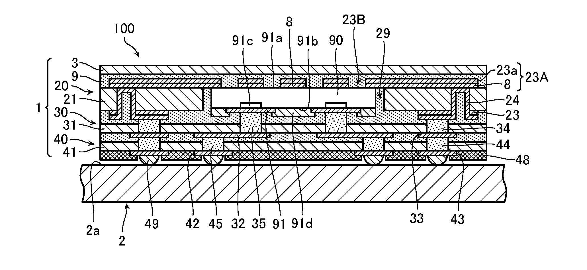
[0046]FIG. 1 is a cross-sectional view showing a structure of a component built-in board mounting body according to a first embodiment of the present invention. As shown in FIG. 1, a component built-in board mounting body 100 according to the first embodiment is configured from a component built-in board 1 and a mounting board 2 on whose mounting surface 2a this component built-in board 1 is mounted.

[0047]The component built-in board 1 comprises a structure in which a second printed wiring base 20, a third printed wiring base 30, a fourth printed wiring base 40, and a cover lay film 3 substituting for a first printed wiring base are stacked collectively by thermal compression bonding. Moreover, the component built-in board 1 comprises an electronic component 90 which is built in to an opening 29 formed in a second resin base 21 of the second printed wiring base 20, in a state of being sandwiched by the third printed wiring base 30 and the cover lay film 3. Furthermore, the component...

second embodiment

[0087]FIG. 13 is a cross-sectional view showing a structure of a component built-in board mounting body according to a second embodiment of the present invention. As shown in FIG. 13, a component built-in board mounting body 100A according to the second embodiment differs from the component built-in board mounting body 100 according to the first embodiment in having a first printed wiring base 10 stacked in place of the cover lay film 3 and in having heat of the electronic component 90 radiated not only from the mounting board 2 but also from a first printed wiring base 10 side.

[0088]Specifically, the first printed wiring base 10 basically can be manufactured by steps similar to those for the fourth printed wiring base 40 described using FIGS. 2 and 6, and is configured from a structure in which the conductor layer 8 having a solid pattern is formed on one surface of the first resin base 11. Different from the fourth printed wiring base 40 is the fact that the conductor layer 8 of t...


PUM

PropertyMeasurementUnit
Electrical conductoraaaaaaaaaa
Heataaaaaaaaaa

Abstract

A component built-in board comprises stacked therein a plurality of printed wiring bases having a wiring pattern and a via formed on/in a resin base thereof, and comprises an electronic component built in thereto, wherein at least a portion of the plurality of printed wiring bases include a thermal wiring in the wiring pattern and include a thermal via in the via, at least one of the plurality of printed wiring bases has formed therein an opening where the electronic component is built, and has formed therein a heat-conducting layer and closely attached to a surface on an opposite side to an electrode formation surface of the electronic component built in to the opening, and the electronic component is fixed in the opening by an adhesive layer stacked on the heat-conducting layer, via a hole formed in a region facing onto the opening of the heat-conducting layer.

Description

CROSS-REFERENCE TO RELATED APPLICATIONS[0001]This application is a continuation application of PCT Application No. PCT / JP2012 / 079463, filed on Nov. 14, 2012, which is based on and claims the benefit of priority from prior Japanese Patent Application No. 2011-262217, filed on Nov. 30, 2011, the entire contents of which are incorporated herein by reference.BACKGROUND OF THE INVENTION[0002]1. Field of the Invention[0003]This invention relates to a component built-in board having an electronic component built in thereto, and a method of manufacturing the same, and to a component built-in board mounting body.[0004]2. Description of the Prior Art[0005]Known to achieve high density mounting of an electronic component is a component built-in board disclosed in Japanese Unexamined Patent Application Publication No. 2008-305937 A which has an electronic component built in to the board. Such a component built-in board has the electronic component buried in an insulating layer formed in a wirin...

Claims


Application Information

Patent Timeline
IPC IPC(8): H05K1/02H05K3/10
CPCH05K3/10H05K1/0206H01L23/5389H05K1/0207H05K1/186H05K3/0061H05K3/4602H05K3/4614H05K2201/0969H05K2201/10674H01L2224/02311H01L23/367H01L23/3677H01L21/4857H01L2224/05569H01L2224/13311H01L2224/80447H01L2224/80903H01L2224/13313H01L2224/1336H01L2224/13316H01L2224/1339H01L2224/11416H01L2224/11418H01L2224/08237H01L2224/0401H01L2224/11312H01L2224/1132H01L2224/11334H01L2224/13009H01L2224/13294H01L2224/13324H01L2224/13339H01L2224/13344H01L2224/13347H01L2224/13355H01L2224/16238H01L2224/2929H01L2224/32225H01L2224/73253H01L2224/81192H01L2224/81203H01L2224/81862H01L2224/81907H01L2224/83192H01L2224/83203H01L2224/8349H01L2224/8385H01L2224/83862H01L2224/9211H01L2224/9221H01L2924/07811H01L2224/80203H01L2224/1329H01L2224/8185H01L2224/16503H01L2224/13309H01L2224/73201H01L2224/73251H01L24/19H01L2224/04105H01L2224/12105H01L2224/16225H01L2924/15153H01L2924/12042Y10T29/49126H01L2924/00014H01L2924/0665H01L2924/0635H01L2924/069H01L2224/81H01L2224/83H01L2224/80H01L2224/16H01L2224/08H01L2224/32H01L2924/00
Inventor ITOI, KAZUHISAOKAMOTO, MASAHIRO
Owner THE FUJIKURA CABLE WORKS LTD
Why Eureka
Try Eureka