Method of manufacturing radiating plate and semiconductor apparatus using the same

Active Publication Date: 2005-10-06
SHINKO ELECTRIC IND CO LTD
View PDF14 Cites 1 Cited by
  • Summary
  • Abstract
  • Description
  • Claims
  • Application Information

AI Technical Summary

Benefits of technology

[0009] Therefore, the invention has been made in order to solve these problems, and it is one of objects in this invention to provide a radiating plate in used of a semiconductor device and its manufacturing methods, which can enhance a thermal conductivity between a semiconductor device and a radiating plate that is bonded to the back surface of the semiconductor device. This is resulting in improvement of the heat radiating characteristics of the radiating plate.
[0010] Further, it is another object of this invention to provide a radiating plate in used of a semiconductor device and its manufacturing method, which enables the radiating plate to keep its thermal conductivity high between the semiconductor device and the radiating plate bonded to the back surface thereof. This is not only improving the heat radiating characteristics of the radiating plate, but also manufacturing the radiating plate more readily, which makes it possible to assemble the semiconductor apparatus more readily.
[0011] Moreover, it is another object of this invention to provide a semiconductor manufacturing methods by using a radiating plate which can alleviate the thermal stress being imposed on the semiconductor device and the radiating plate in case of the both being bonded together. This method is resulting in significant reduce of the damage given to the semiconductor device.

Problems solved by technology

If the thermal conductor is heated and molten to bond the semiconductor device 12 to the radiating plate 14 with high temperature, however, there is a possibility of causing a great thermal stress between the substrate 10 and the semiconductor device 12, as well as between the radiating plate 14 and the semiconductor device 12, resulting in the damage of the semiconductor device 12.
As in the case in which the solder is used as the thermal conductor, moreover, if the thermal conductor is molten to bond the semiconductor device 12 to the radiating plate 14, there is a problem of the generated voids remaining between the back surface of the semiconductor device 12 and the radiating plate 14, which does not fill up the clearance portion completely, resulting in tampering a thermal conductivity in some cases.
On the other hand, in the case in which the high-temperature conducting resin is used as the thermal conductor, giving the priority to good filling condition of the thermal conductor, there is a problem of the thermal conductivity turning to be lower in comparison of a metal material such as the solder.

Method used


Image

  • Method of manufacturing radiating plate and semiconductor apparatus using the same
  • Method of manufacturing radiating plate and semiconductor apparatus using the same
  • Method of manufacturing radiating plate and semiconductor apparatus using the same

Examples


first embodiment

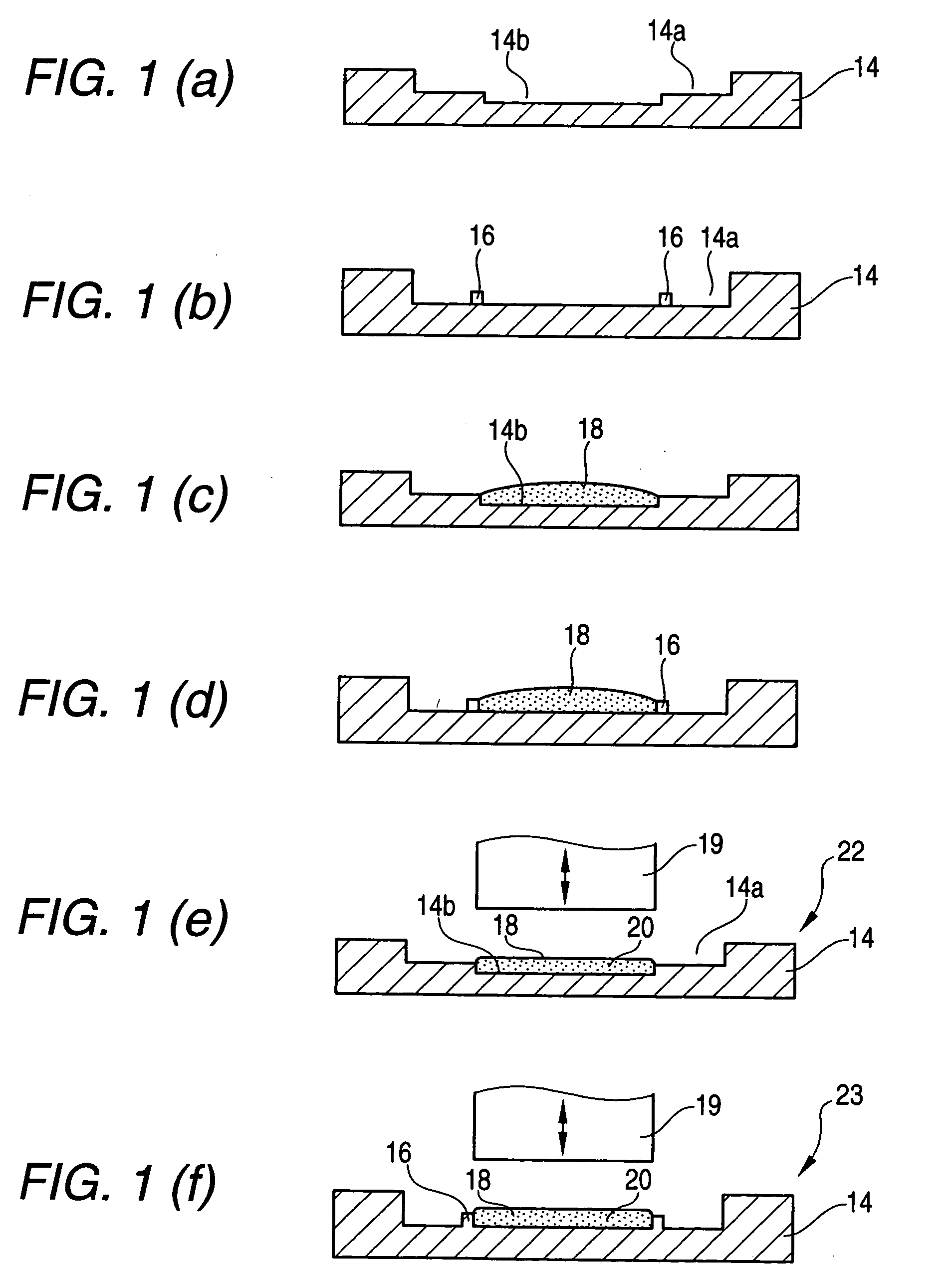
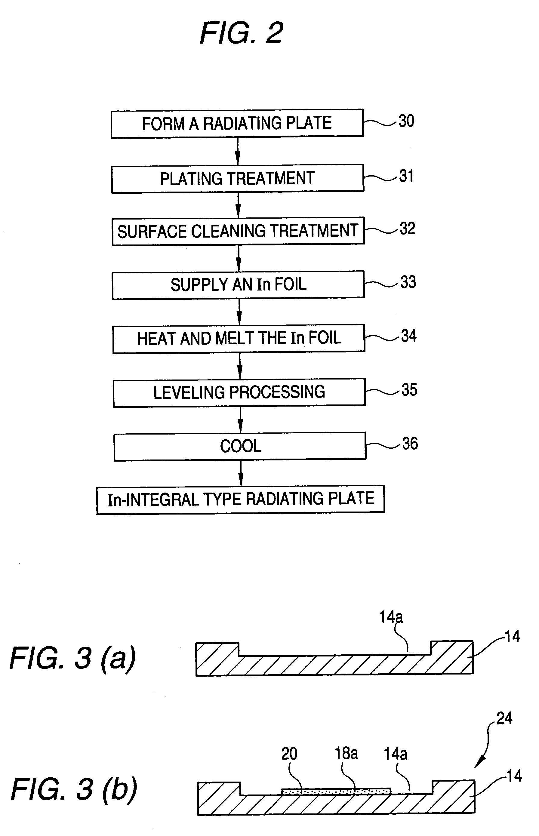
[0032] FIGS. 1(a) to 1(f) are the explanatory views showing a process for manufacturing a radiating plate according to the invention and FIG. 2 is a flowchart showing a manufacturing process according to a first embodiment.

[0033] FIGS. 1(a) and 1(b) show a state in which a radiating plate 14 is formed to take a predetermined shape at a radiating plate forming step 30 using a press processing shown in FIG. 2.

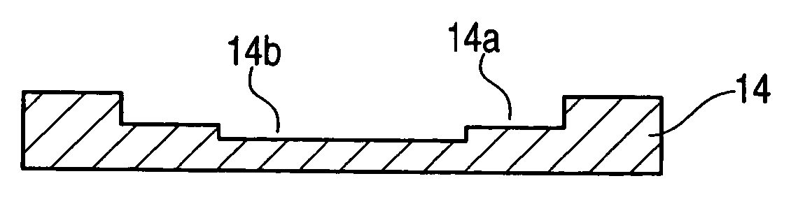
[0034]FIG. 1(a) shows a state in which a housing concave portion 14a is formed on the base material of the radiating plate 14 and a concave portion 14b is formed in the central part of the housing concave portion 14a. Both the housing concave portion 14a and the concave portion 14b take a rectangular planar shape in the embodiment.

[0035]FIG. 1(b) shows another example of the structure of the radiating plate 14, in which the housing concave portion 14a is formed on a base material by a press processing and a resin material such as an epoxy resin is then applied like a frame ont...

second embodiment

[0052] In the method of manufacturing an In integral type radiating plate according to the embodiment described above, the In foil is heated and molten and the In-containing thermal conducting bonding material 20 is adhered integrally with the radiating plate 14. Second and third embodiments which will be described below are characterized in that it is possible to obtain the In integral type radiating plate, having the radiating plate 14 and the In foil integrated with each other, by only causing the In foil to come in contact with the radiating plate 14 under room temperature as it is without need of heating and melting the In foil.

[0053] FIGS. 3(a) and 3(b) show the structures of the radiating plate 14 to be used in the second embodiment. In the second embodiment, an In foil is exactly adhered to the radiating plate 14 and the In foil and the radiating plate 14 are thus integrated with each other. For this reason, it is not necessary to provide a concave portion 14b and a barrier...

third embodiment

[0067] While the first plating and the second plating are carried out over the radiating plate 14 and the electrolytic treatment utilizing an electrolyte is then performed as the surface cleaning treatment for the radiating plate 14 in the second embodiment, a third embodiment is characterized in that a sulfuric acid solution is used to carry out the surface cleaning treatment for the radiating plate 14.

[0068] Since the structure of the radiating plate 14 and the contents of treatments in a first plating step 37 and a second plating step 38 are completely identical to those in the second embodiment, description will be omitted.

[0069] At a surface cleaning step 39 in the embodiment, the radiating plate 14 subjected to the first plating and the second plating is immersed in 1N sulfuric acid, and subsequently, an In foil is immersed in a dilute sulfuric acid solution and is put stationarily for 30 seconds or more, and the In foil is then pressed against the radiating plate 14 so that...


PUM


Abstract

A method of manufacturing a radiating plate using In as a thermal conducting bonding material 20 provided between a semiconductor device and a radiating plate 14 and serving to bond a back surface of the semiconductor device to the radiating plate, includes the steps of carrying out a cleaning treatment for cleaning a surface of the radiating plate 14, supplying the In to the radiating plate 14, heating and melting the In and hermetically adhering the In 18 to the radiating plate, thereby obtaining an In integral type radiating plate.

Description

BACKGROUND OF THE INVENTION [0001] 1. Field of the Invention [0002] The present invention relates to a method of manufacturing a radiating plate and a semiconductor apparatus using the radiating plate. [0003] 2. Description of the Related Art [0004] In a semiconductor apparatus mounting a semiconductor device by a flip chip connection, a radiating plate is attached to the back surface of the semiconductor device (a surface on an opposite side to the flip chip connecting surface of the semiconductor device) to enhance the thermal radiating property thereof. FIG. 7 shows an example of a semiconductor apparatus formed by flip chip connecting a semiconductor device 12 to a substrate 10 with bonding a radiating plate 14 to the back surface of the semiconductor device 12. In this example, the radiating plate 14 is provided with a housing concave portion 14a for accommodating the semiconductor device 12 and the semiconductor device 12 is bonded to the inner bottom surface (or ceiling surfa...

Claims


Application Information

Patent Timeline
IPC IPC(8): H01L23/40H01L21/44H01L21/48H01L21/50H01L23/34H01L23/36H01L23/373
CPCH01L21/4882H01L23/3736H01L2224/16H01L2224/73253H01L2924/01046H01L2924/01078H01L2924/01079H01L2924/15311H01L2924/16152H01L2924/01019
Inventor AKAGAWA, MASATOSHINAKAZAWA, MASAONAKAZAWA, HIDETO
Owner SHINKO ELECTRIC IND CO LTD
Why Eureka
Try Eureka