
Component built-in board mounting body and method of manufacturing the same, and component built-in board

a technology of built-in components and mounting bodies, which is applied in the direction of printed element electric connection formation, printed circuit non-printed electric components association, semiconductor/solid-state device details, etc., can solve the problems of insufficient heat radiation characteristics of electronic components, inability to say that the structure is sufficiently responding to the requirements of miniaturization, and increase in overall height, so as to improve the heat radiation characteristics of built-in electronic components. , the flexibility

Active Publication Date: 2017-04-25
FUJIKURA LTD
View PDF21 Cites 0 Cited by
  • Summary
  • Abstract
  • Description
  • Claims
  • Application Information

AI Technical Summary

Benefits of technology

This solution enhances heat radiation characteristics while achieving miniaturization and increasing layout flexibility by directly connecting the electronic component to the mounting board through thermal vias and wiring, providing a more effective heat radiation path without the need for a conventional heat radiation board.

Problems solved by technology

Hence, it cannot say that heat radiation characteristics of the electronic component have been sufficiently improved, and there is room for further improvement in heat radiation characteristics to be achieved.
Hence, for example, when mounted on a mounting board, overall height increases and it cannot say that the structure is sufficiently responding to the requirements of miniaturization, and so on.
Hence, there is a problem that flexibility of layout of the electronic component is limited.

Method used


Image

  • Component built-in board mounting body and method of manufacturing the same, and component built-in board
  • Component built-in board mounting body and method of manufacturing the same, and component built-in board
  • Component built-in board mounting body and method of manufacturing the same, and component built-in board

Examples


first embodiment

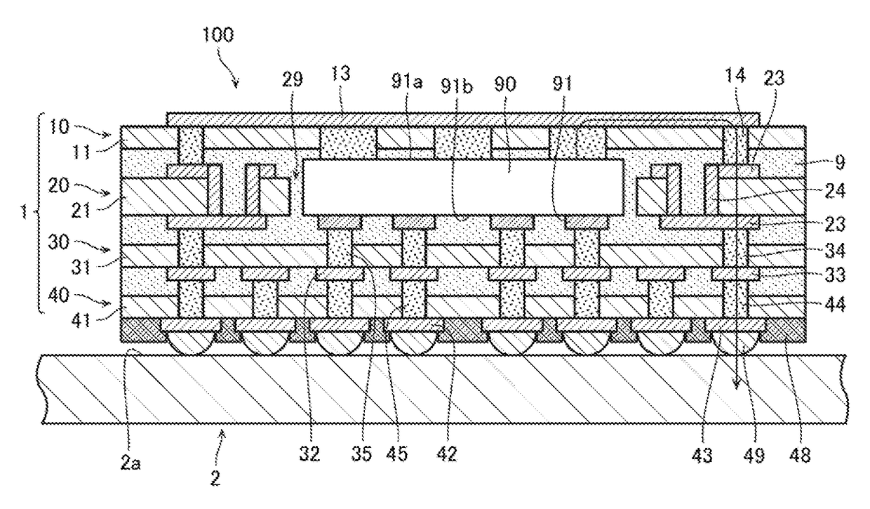
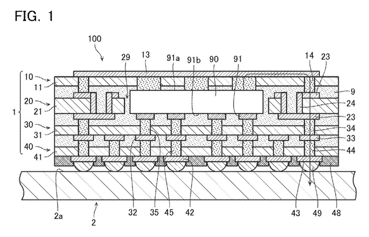
[0043]FIG. 1 is a cross-sectional view showing a structure of a component built-in board mounting body according to a first embodiment of the present invention. As shown in FIG. 1, a component built-in board mounting body 100 according to the first embodiment is configured from a component built-in board 1 and a mounting board 2 on a mounting surface 2a of which the component built-in board 1 is mounted.

[0044]The component built-in board 1 comprises a structure in which a first printed wiring base 10, a second printed wiring base 20, a third printed wiring base 30, and a fourth printed wiring base 40 are stacked collectively by thermal compression bonding. Moreover, the component built-in board 1 comprises an electronic component 90 which is built in to an opening 29 formed in a second resin base 21 of the second printed wiring base 20, in a state of being sandwiched by the first and third printed wiring bases 10 and 30. Furthermore, the component built-in board 1 comprises a bump 4...

second embodiment

[0064]FIG. 4 is a cross-sectional view showing a structure of a component built-in board mounting body according to a second embodiment of the present invention. As shown in FIG. 4, a component built-in board mounting body 200 according to the second embodiment differs from the component built-in board mounting body 100 according to the first embodiment in having the component built-in board 1 mounted face up (up and down reversed) on the mounting surface 2a of the mounting board 2, and in having a connection mode of the signal-dedicated wiring lines and thermal wiring lines of each of the printed wiring bases 10 to 40 changed due to a pattern of the thermal wiring line 13 of the first printed wiring base 10 being changed.

[0065]That is, in this component built-in board mounting body 200, solder resist 48 pattern-formed on the first resin base 11 on a thermal wiring line 13 side of the first printed wiring base 10 in the component built-in board 1 is provided, the bump 49 is formed o...

third embodiment

[0067]FIG. 5 is a cross-sectional view showing a structure of a component built-in board mounting body according to a third embodiment of the present invention. A component built-in board mounting body 300 according to the third embodiment differs from the component built-in board mounting body 200 according to the second embodiment in having an electronic component 98 (second electronic component) further surface-mounted on the component built-in board mounting body 200 according to the second embodiment having the electronic component 90 (first electronic component) built in thereto.

[0068]That is, as shown in FIG. 5, in this component built-in board mounting body 300, a first bump 49 is formed on the signal-dedicated wiring line 12 and the thermal wiring line 13 of the first printed wiring base 10 in the component built-in board 1, and the solder resist 48 pattern-formed on the fourth resin base 41 on a signal-dedicated wiring line 42 side of the fourth printed wiring base 40 is f...


PUM

PropertyMeasurementUnit
temperatureaaaaaaaaaa
thicknessaaaaaaaaaa

Abstract

A component built-in board mounting body has a component built-in board mounted on a mounting board, the component built-in board being configured having stacked therein a plurality of printed wiring bases that each have a wiring pattern and a via formed on / in a resin base thereof, and having an electronic component built in thereto, wherein the component built-in board has at least a portion of the plurality of printed wiring bases including thermal wiring in the wiring pattern and including a thermal via in the via, and is mounted on the mounting board via a bump formed on a surface layer of the component built-in board, and a surface on an opposite side to an electrode formation surface of the built in electronic component is connected to the bump via the thermal via and the thermal wiring, and is thermally connected to the mounting board via the bump.

Description

CROSS-REFERENCE TO RELATED APPLICATIONS[0001]This application is a continuation application of PCT Application No. PCT / JP2012 / 074562, filed on Sep. 25, 2012, which is based on and claims the benefit of priority from prior Japanese Patent Application No. 2011-216527, filed on Sep. 30, 2011, the entire contents of which are incorporated herein by reference.BACKGROUND OF THE INVENTION[0002]Field of the Invention[0003]This invention relates to a component built-in board mounting body in which a component built-in board having an electronic component built in thereto is mounted on a mounting board, and a method of manufacturing the same, and to a component built-in board.[0004]Description of the Prior Art[0005]In recent years, miniaturization or higher levels of integration are being required in electronic components of semiconductors and the like, and there is a tendency to increasingly adopt three-dimensional packaging technology such as CoC (Chip on Chip) and PoP (Package on Package),...

Claims


Application Information

Patent Timeline
Patent Type & Authority Patents(United States)
IPC IPC(8): H05K1/18H01L23/538H05K3/30H05K1/02H01L23/367H01L23/31H05K3/40H05K3/00H05K3/46H01L23/498H05K3/42
CPCH05K1/185H01L23/3121H01L23/3677H01L23/49833H01L23/5389H05K1/0206H05K1/0298H05K1/186H05K3/301H01L23/49816H01L2224/16225H01L2224/32225H01L2224/73204H01L2924/01327H05K3/0026H05K3/4038H05K3/4053H05K3/429H05K3/462H05K3/4614H05K3/4617H05K3/4623H05K2203/1453Y10T29/4913H01L2924/00
Inventor UETA, NOBUKI
Owner FUJIKURA LTD
Learn More