Integrated circuit system with non-volatile memory stress suppression and method of manufacture thereof

a non-volatile memory and integrated circuit technology, applied in the field of integrated circuit systems, can solve the problems of conflicting requirements of the integrated circuit industry, damage to the thinner crystalline structure or memory leakage through the physical structure, and limited production, so as to reduce the voltage excursion of the bit line

Active Publication Date: 2014-09-18
SONY SEMICON SOLUTIONS CORP
View PDF13 Cites 10 Cited by
  • Summary
  • Abstract
  • Description
  • Claims
  • Application Information

AI Technical Summary

Benefits of technology

[0009]The present invention provides a method of manufacture of an integrated circuit system including: providing an integrated circuit die; forming a non-volatile memory cell in the integrated circuit die and having a bit line for reading a data condition state of the non-volatile memory cell; and forming a voltage clamp in the integrated circuit die, the voltage clamp having a semiconductor switch connected to the bit line for reducing voltage excursions on the bit line.

Problems solved by technology

The trend for including ever-increasing amounts of memory in these devices with faster access and performance needs has presented challenges to the integrated circuit industry that impose conflicting requirements on the integrated circuits.
However, the pursuit for faster performing non-volatile memory having thinner crystalline structures associated with smaller geometry technologies often results in damage of the thinner crystalline structure or memory leak through of the physical structures.
While these technologies show promise and these mechanisms can be utilized on any of the small geometry technologies, they have similar problems in terms of reliability and robustness resulting in limited production which prevents these technologies from reaching commodity status.
Solutions to these problems have been long sought but prior developments have not taught or suggested any solutions and, thus, solutions to these problems have long eluded those skilled in the art.

Method used


Image

  • Integrated circuit system with non-volatile memory stress suppression and method of manufacture thereof
  • Integrated circuit system with non-volatile memory stress suppression and method of manufacture thereof
  • Integrated circuit system with non-volatile memory stress suppression and method of manufacture thereof

Examples


Embodiment Construction

[0026]The following embodiments are described in sufficient detail to enable those skilled in the art to make and use the invention. It is to be understood that other embodiments would be evident based on the present disclosure, and that system, process, or mechanical changes may be made without departing from the scope of the present invention.

[0027]In the following description, numerous specific details are given to provide a thorough understanding of the invention. However, it will be apparent that the invention may be practiced without these specific details. In order to avoid obscuring the present invention, some well-known circuits, system configurations, and process steps are not disclosed in detail.

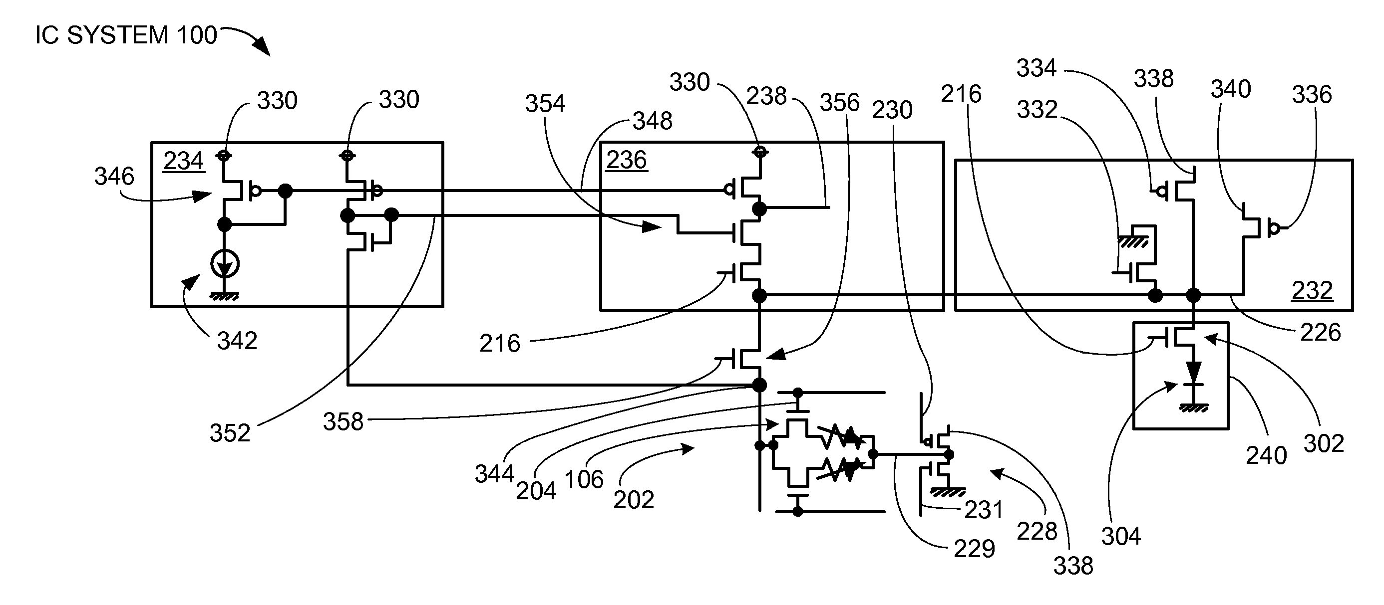
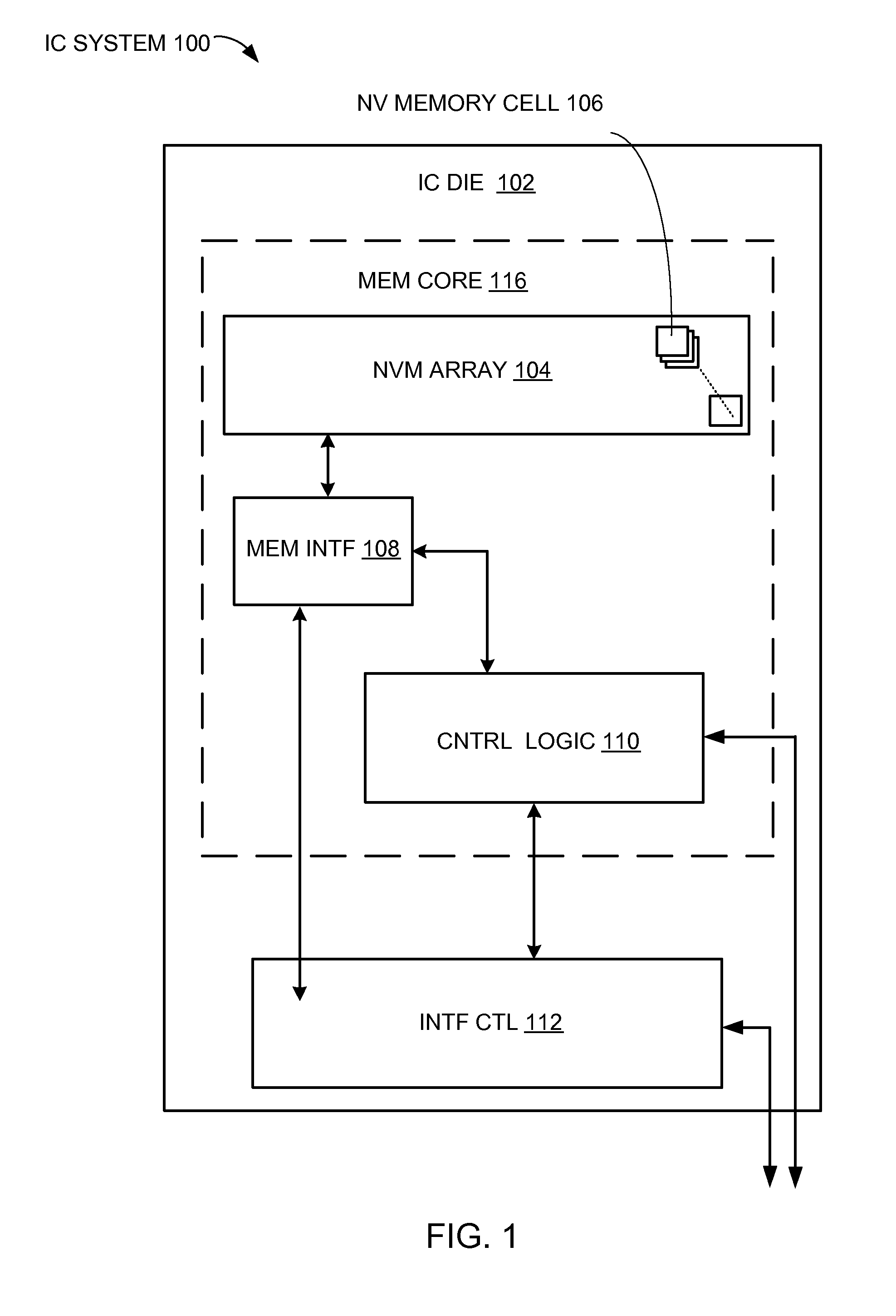
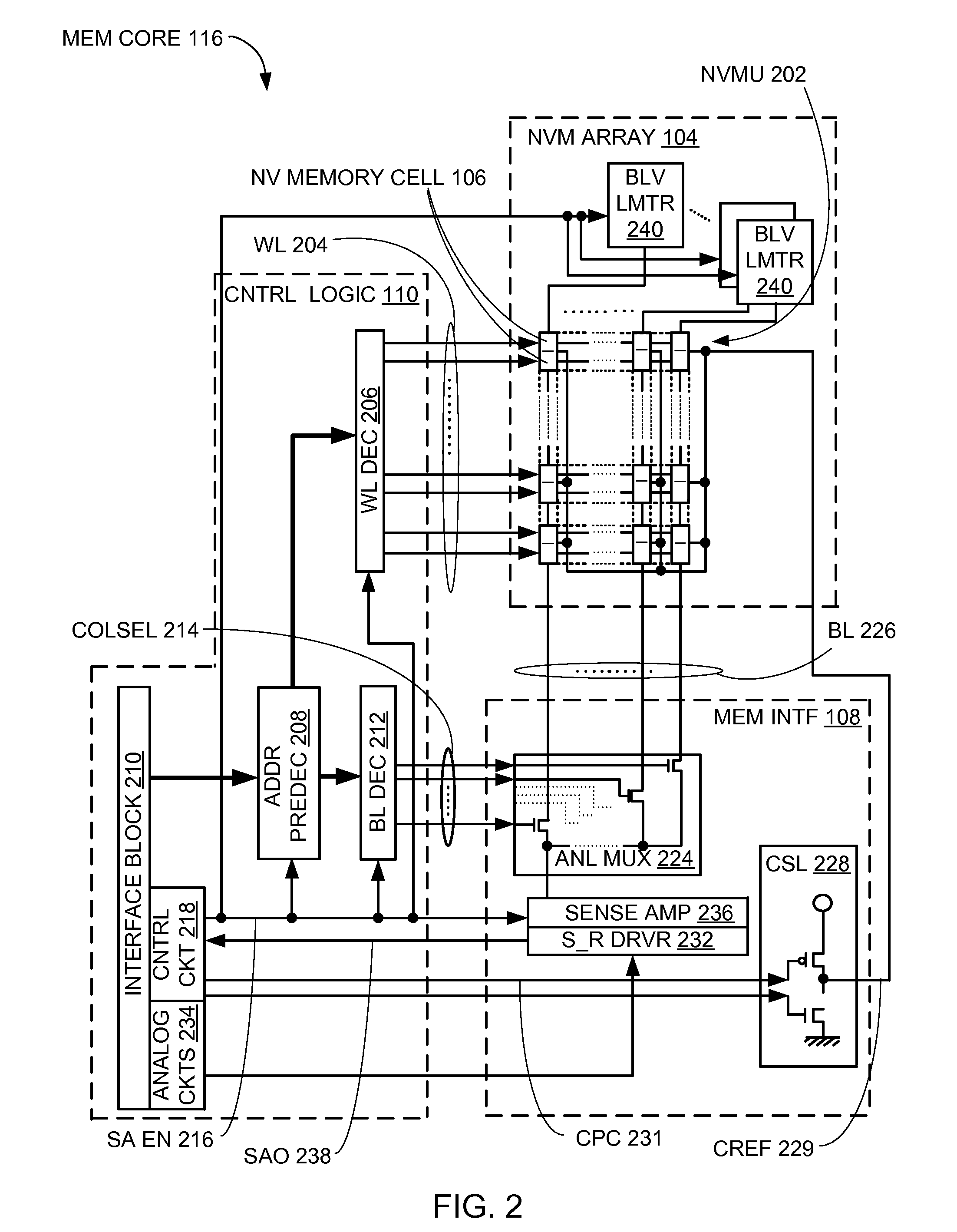
[0028]The schematic drawings are depicted based on an electron flow current convention. The drawings showing embodiments of the system are semi-diagrammatic and not to scale and, particularly, some of the dimensions are for the clarity of presentation and are shown exaggerated in ...


PUM


Abstract

An integrated circuit system, and a method of manufacture thereof, including: an integrated circuit die; a non-volatile memory cell in the integrated circuit die and having a bit line for reading a data condition state of the non-volatile memory cell; and a voltage clamp in the integrated circuit die, the voltage clamp having a semiconductor switch connected to the bit line for reducing voltage excursions on the bit line.

Description

TECHNICAL FIELD[0001]The present invention relates generally to an integrated circuit system, and more particularly to a system for integration of high-density non-volatile memory arrays in integrated circuit applications.BACKGROUND ART[0002]The trend for including ever-increasing amounts of memory in these devices with faster access and performance needs has presented challenges to the integrated circuit industry that impose conflicting requirements on the integrated circuits. In order to accommodate the increased amount of logic and memory, smaller and smaller geometries are required to contain the functions.[0003]Memories such as non-volatile Flash memory or dynamic random access memory (DRAM) maintain the data content by storing charge within a physical structure in the memory cell. However, the pursuit for faster performing non-volatile memory having thinner crystalline structures associated with smaller geometry technologies often results in damage of the thinner crystalline s...

Claims


Application Information

Patent Timeline
Patent Type & Authority Applications(United States)
IPC IPC(8): G11C5/06
CPCG11C5/063G11C7/12G11C7/18
Inventor KITAGAWA, MAKOTOTSUSHIMA, TOMOHITOOTSUKA, WATARUKUNIHIRO, TAKAFUMI
Owner SONY SEMICON SOLUTIONS CORP
Why Eureka
Try Eureka