Method for driving semiconductor device and semiconductor device
a technology of semiconductor devices and semiconductor chips, applied in semiconductor devices, digital storage, instruments, etc., can solve the problem of long time required for data reading
Active Publication Date: 2014-09-18
SEMICON ENERGY LAB CO LTD
View PDF5 Cites 28 Cited by
- Summary
- Abstract
- Description
- Claims
- Application Information
AI Technical Summary
Benefits of technology
The present invention offers a method for reading data from a semiconductor device with a unique structure that allows for multiple levels of data without needing to switch signals for each level. This results in faster and more efficient data reading.
Problems solved by technology
In such a structure, the larger the number of the levels of the multilevel data is, the larger the number of times the voltage level of the read signal needs to be switched; accordingly, reading of data takes a long time.
Method used
View moreImage
Smart ImageViewing Examples
Examples
embodiment 1 (
1. Embodiment 1 (memory cell according to one embodiment of the present invention)
embodiment 2 (
2. Embodiment 2 (configuration example of semiconductor device)
embodiment 3 (
3. Embodiment 3 (oxide semiconductor)
4. Embodiment 4 (elements of semiconductor device)
Login to View More PUM
 Abstract
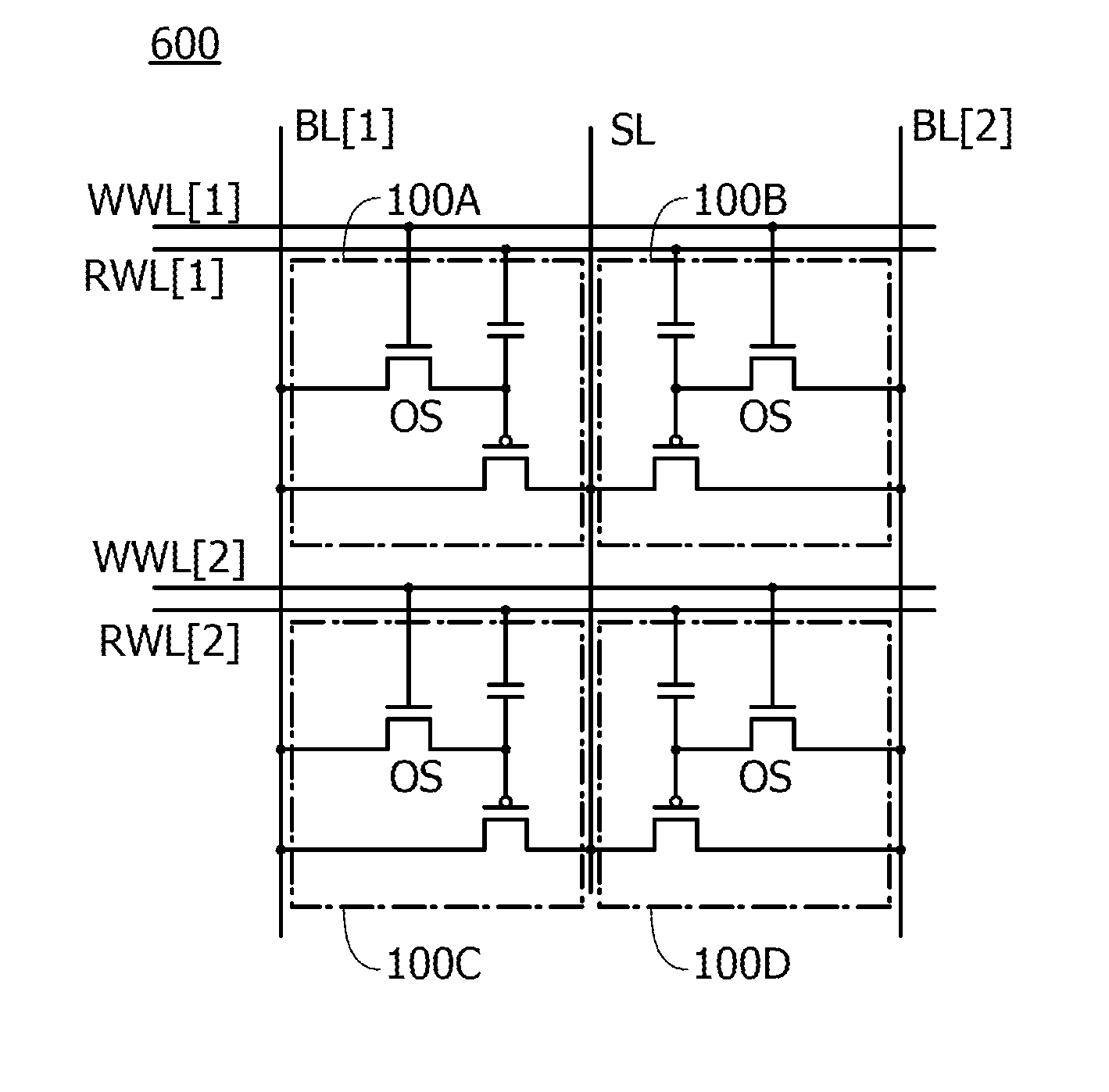
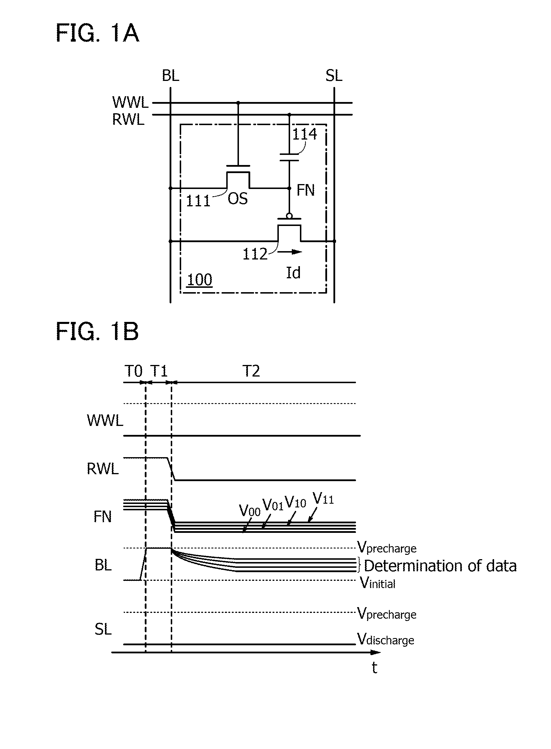
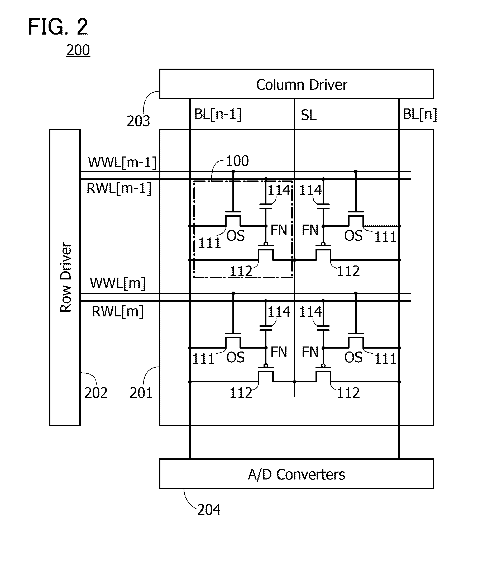
To read multilevel data from a memory cell having a transistor using silicon and a transistor using an oxide semiconductor, without switching a signal for reading the multilevel data in accordance with the number of the levels of the multilevel data. The potential of the bit line is precharged, the electrical charge of the bit line is discharged via a transistor for writing data, and the potential of the bit line which is changed by the discharging is read as multilevel data. With such a structure, the potential corresponding to data held in a gate of the transistor can be read by only one-time switching of a signal for reading data.
Description
TECHNICAL FIELD[0001]The present invention relates to a method for driving a semiconductor device.BACKGROUND ART[0002]A semiconductor device capable of holding data that includes a transistor whose semiconductor layer is formed using silicon (Si) and a transistor whose semiconductor layer is formed using an oxide semiconductor (OS) has attracted attention (see Patent Document 1).[0003]In recent years, with the increase in the amount of data manipulated, a semiconductor device having a large storage capacity has been required. In such situations, the semiconductor device disclosed in Patent Document 1 has a structure in which multilevel data is stored and read.REFERENCEPatent Document[0004][Patent Document 1] Japanese Published Patent Application No. 2012-256400DISCLOSURE OF INVENTION[0005]In the case where multilevel data is read from a memory cell, a signal for reading data needs to be switched two or more times in accordance with the number of levels of the multilevel data.[0006]F...
Claims
Login to View More Application Information
Patent Timeline
 Patent Type & Authority Applications(United States)
IPC IPC(8): G11C16/24
CPCG11C16/24G11C11/5642G11C16/08H01L29/7869H01L29/78696H01L27/1225H10B41/70G11C16/0441G11C16/04G11C16/045G11C16/0408
Inventor NAGATSUKA, SHUHEIINOUE, HIROKIISHIZU, TAKAHIKOMATSUZAKI, TAKANORISHIONOIRI, YUTAKAKATO, KIYOSHI
Owner SEMICON ENERGY LAB CO LTD


