Input buffer apparatuses and methods

a buffer and input technology, applied in the field of input buffer apparatuses and methods, can solve the problems of loss of gain, affecting the capacity of mos-based self-biased differential amplifiers, and affecting the layout area and power requirements of substantial size and power requirements,

Active Publication Date: 2014-09-18
MICRON TECH INC
View PDF6 Cites 32 Cited by
  • Summary
  • Abstract
  • Description
  • Claims
  • Application Information

AI Technical Summary

Problems solved by technology

However, as the frequency of the input signal approaches 1 GHz, the gain of the MOS-based self-biased differential amplifier can roll off.
This loss in gain can compromise the capacity of the MOS-based self-biase

Method used


Image

  • Input buffer apparatuses and methods
  • Input buffer apparatuses and methods
  • Input buffer apparatuses and methods

Examples


Embodiment Construction

[0011]For the purposes of this document, an “apparatus” can refer to any of a number of structures, such as circuitry, a device or a system. In this description, a transistor is described as being switched on to assume an activated state when it is rendered conductive by a control gate voltage. The transistor is described as being switched off to assume an inactive state when it is rendered non-conductive by a control gate voltage. Potentials refer to electrical potentials.

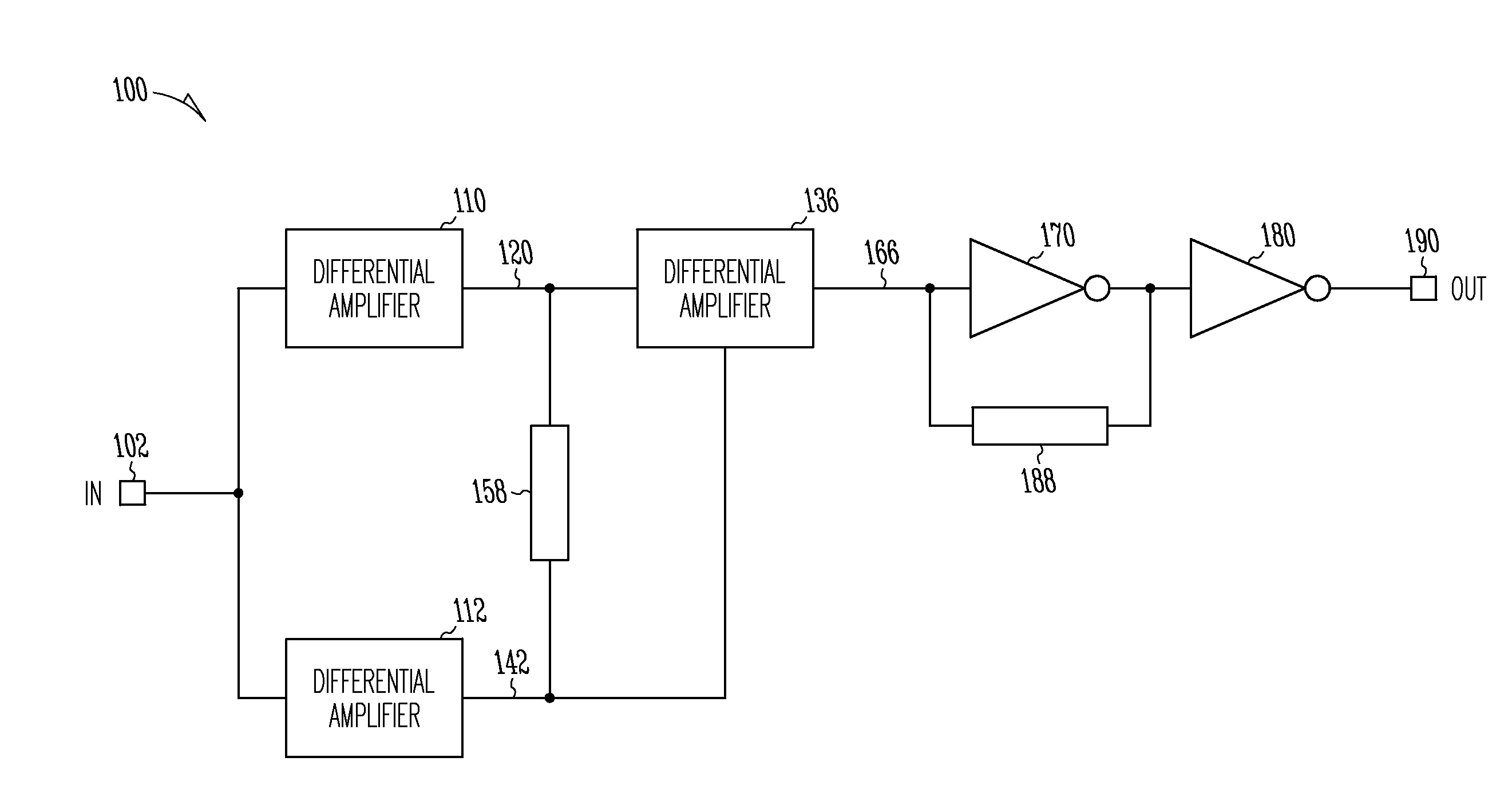
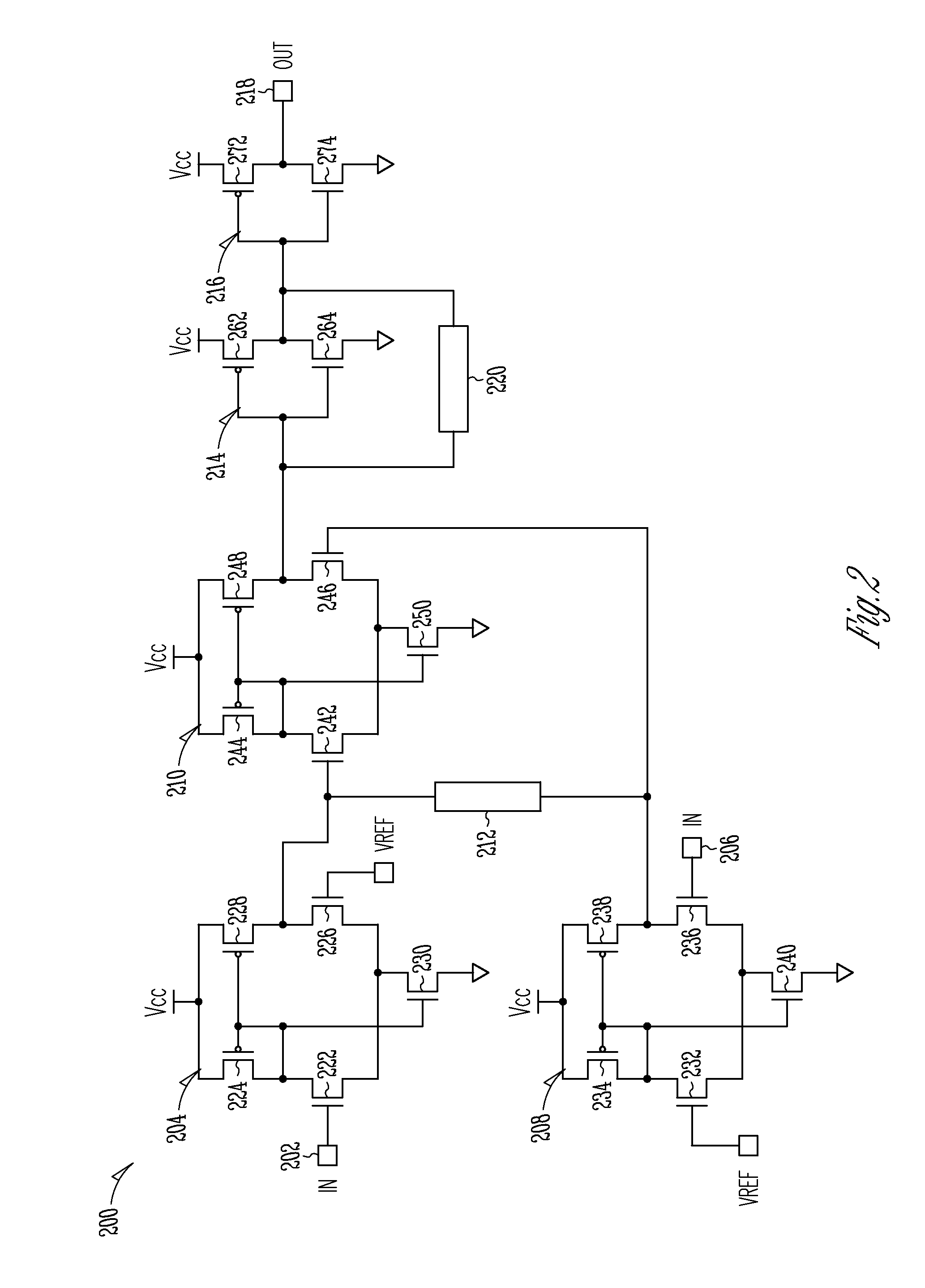
[0012]The challenges noted above, as well as others, can be addressed by an apparatus shown in FIG. 1. FIG. 1 is a block diagram of an apparatus in the form of an input buffer system 100 according to various embodiments. An input signal IN is received at an input terminal 102 coupled to inputs of a first differential amplifier 110 and a second differential amplifier 112. The first differential amplifier 110 amplifies the input signal IN to generate a first output signal on a first output line 120 that is coupled t...


PUM


Abstract

Apparatuses and methods are disclosed, including an apparatus with a first differential amplifier to amplify an input signal into a first output signal, a second differential amplifier to amplify the input signal into a second output signal that is complementary to the first output signal, and a feedback resistance coupled between the first output signal and the second output signal. Additional apparatuses and methods are described.

Description

BACKGROUND[0001]Integrated circuit devices can have input buffers to convert analog data input signals into full-rail complementary metal-oxide-semiconductor (CMOS) signals. For single-ended input signals, the transition from a logic ‘high’ to a logic ‘low’ is dependent on when the input signal crosses a reference voltage. A differential amplifier may detect the transition of the input signal across the reference voltage.[0002]A metal-oxide-semiconductor (MOS)-based self-biased differential amplifier can convert input signal swings of less than 100 millivolts to full-rail signals. However, as the frequency of the input signal approaches 1 GHz, the gain of the MOS-based self-biased differential amplifier can roll off. This loss in gain can compromise the capacity of the MOS-based self-biased differential amplifier to convert the input signal into a full-rail output signal.[0003]Current Mode Logic (CML) input buffers can be used for an input-output (I / O) interface. CML input buffers a...

Claims


Application Information

Patent Timeline
IPC IPC(8): G11C7/10H03F3/45
CPCH03F3/45179G11C7/1084H03F3/45183H03F2203/45051
Inventor TAYLOR, JENNIFERDIMITRIU, DRAGOS
Owner MICRON TECH INC
Why Eureka
Try Eureka