Semiconductor device manufacturing method

Inactive Publication Date: 2014-09-25
SEIKO EPSON CORP
View PDF5 Cites 5 Cited by
  • Summary
  • Abstract
  • Description
  • Claims
  • Application Information

AI Technical Summary

Benefits of technology

The patent describes a method for reducing the size of semiconductor devices by diffusing impurities in two stages. By first diffusing the impurities in a first layer, followed by a second process to diffuse the impurities in a second layer, the thermal process time is reduced and the area of the device is minimized.

Problems solved by technology

In this structure, reduction of an element area is a problem to be solved.

Method used


Image

  • Semiconductor device manufacturing method
  • Semiconductor device manufacturing method
  • Semiconductor device manufacturing method

Examples


Embodiment Construction

[0022]The following is a detailed description of embodiments of the invention. Note that the embodiments described below are not intended to unduly limit the content of the invention recited in the claims, and all of the configurations described in the embodiments are not necessarily essential as solutions provided by the invention. Also, similar constituent elements are provided the same reference sign, and redundant description thereof will be omitted.

[0023]1. Configuration

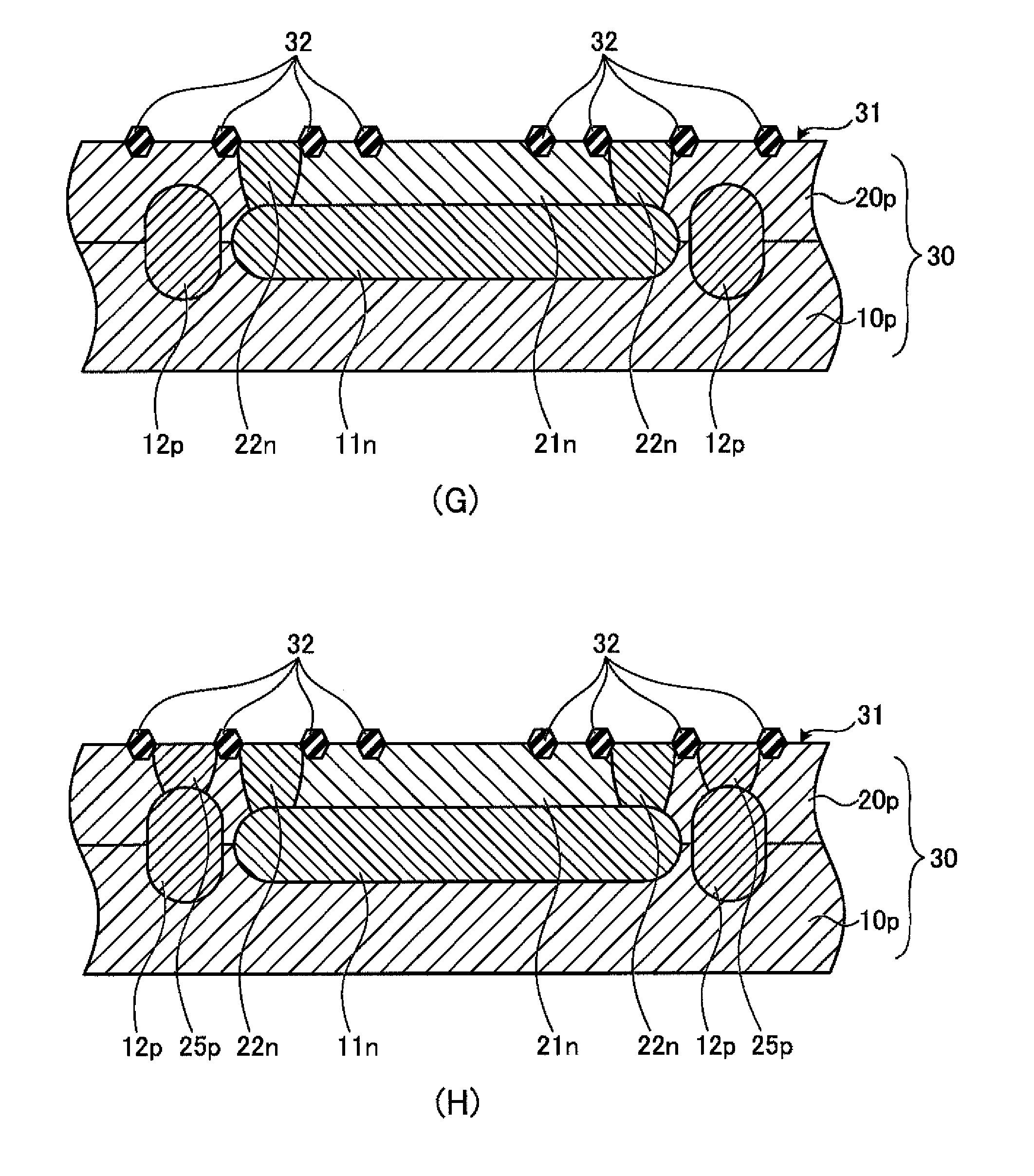
[0024]FIG. 1 is a cross-section showing an example of a semiconductor device manufactured by the manufacturing method according to an embodiment of the present invention. A semiconductor device 1 shown in FIG. 1 includes a first buried diffusion layer 11n, a first impurity region 21n, a second impurity region 22n, a second buried diffusion layer 12p, and a fifth impurity region 25p in a semiconductor substrate 30 that has a base layer 10p and an epitaxial layer 20p. In the description of this embodiment, referen...


PUM


Abstract

A semiconductor device manufacturing method includes (a) forming a buried diffusion layer of a first conductivity type in a semiconductor substrate of a second conductivity type, (b) forming a first impurity region by implanting an impurity of the first conductivity type, (c) diffusing the buried diffusion layer and the first impurity region to an extent that the buried diffusion layer and the first impurity region are not connected by performing a first thermal process on the semiconductor substrate, (d) forming a second impurity region by implanting an impurity of the first conductivity type at a concentration higher than that of in step (b), and (e) diffusing the buried diffusion layer, the first impurity region, and the second impurity region by performing a second thermal process on the semiconductor substrate.

Description

[0001]The entire disclosure of Japanese Patent Application No. 2013-062056, filed Mar. 25, 2013 is expressly incorporated by reference herein.BACKGROUND[0002]1. Technical Field[0003]The present invention relates to a semiconductor device manufacturing method.[0004]2. Related Art[0005]In order to manufacture DMOS (Double Diffused Metal Oxide Semiconductor) transistors or bipolar transistors, a first impurity region that is connected to a buried diffusion layer and a second impurity region that is connected to the buried diffusion layer are formed. For example, a bottom of a well (first impurity region) in which DMOS transistors or bipolar transistors are formed is limited by a buried diffusion layer, and an outer circumference of the well is limited by plugs (second impurity region). In this structure, reduction of an element area is a problem to be solved.[0006]JP-A-10-284731 (FIGS. 7 to 10 and paragraphs 0021 to 0023) describes a situation in which, in order to form a drain region,...

Claims


Application Information

Patent Timeline
IPC IPC(8): H01L21/265
CPCH01L21/265H01L21/26513H01L29/66681H01L29/7823H01L21/761H01L21/74H01L21/823481H01L29/7322
Inventor FURUHATA, TOMOYUKI
Owner SEIKO EPSON CORP
Why Eureka
Try Eureka