Semiconductor device and method of manufacturing the same

Inactive Publication Date: 2012-03-15
ABLIC INC
View PDF2 Cites 4 Cited by
  • Summary
  • Abstract
  • Description
  • Claims
  • Application Information

AI Technical Summary

Benefits of technology

[0011]It is an object of the present invention to provide a semiconductor device including a vertical MOSFET and a method of manufacturing the semiconductor device, which are capable of performing stable processing without increasing the number of manufacturing steps.
[0015]According to the present invention, while leaving the silicon nitride film used to form the trench on the surface of the semiconductor substrate, the gate electrode material buries the trench, and then the gate electrode material on the silicon nitride film is removed, to thereby form the gate electrode inside the trench. As a result the upper end portion of the gate electrode material is never formed below the surface of the semiconductor substrate when the gate electrode material is removed, if the over-etching amount does not exceed the thickness of the silicon nitride film. Accordingly, characteristic fluctuations of the semiconductor device caused by the etching process of the gate electrode material are reduced. Further, since the upper portion of the gate electrode is shaped into an I-shape having the same width as the trench width and not shaped into a T-shape having a width longer than the trench width according to the manufacturing steps of the present invention, not only reduction in element area is achieved but also photolithography for forming the T-shape becomes unnecessary.

Problems solved by technology

However, in this method, fluctuations in etch-back directly cause change in channel length of the MOSFET, and hence there is a fear that manufacturing yield decreases.
However, the number of manufacturing steps increases compared to that of the former case, and the element area increases, causing increase in unit price per chip, which leads to a cost problem.

Method used


Image

  • Semiconductor device and method of manufacturing the same
  • Semiconductor device and method of manufacturing the same
  • Semiconductor device and method of manufacturing the same

Examples


Embodiment Construction

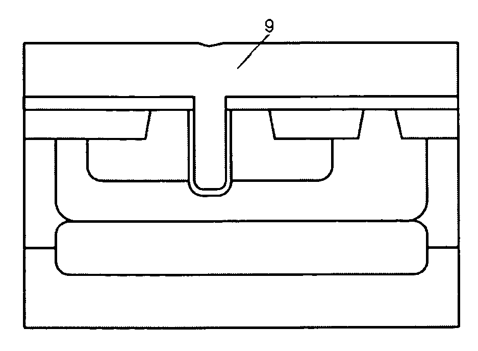
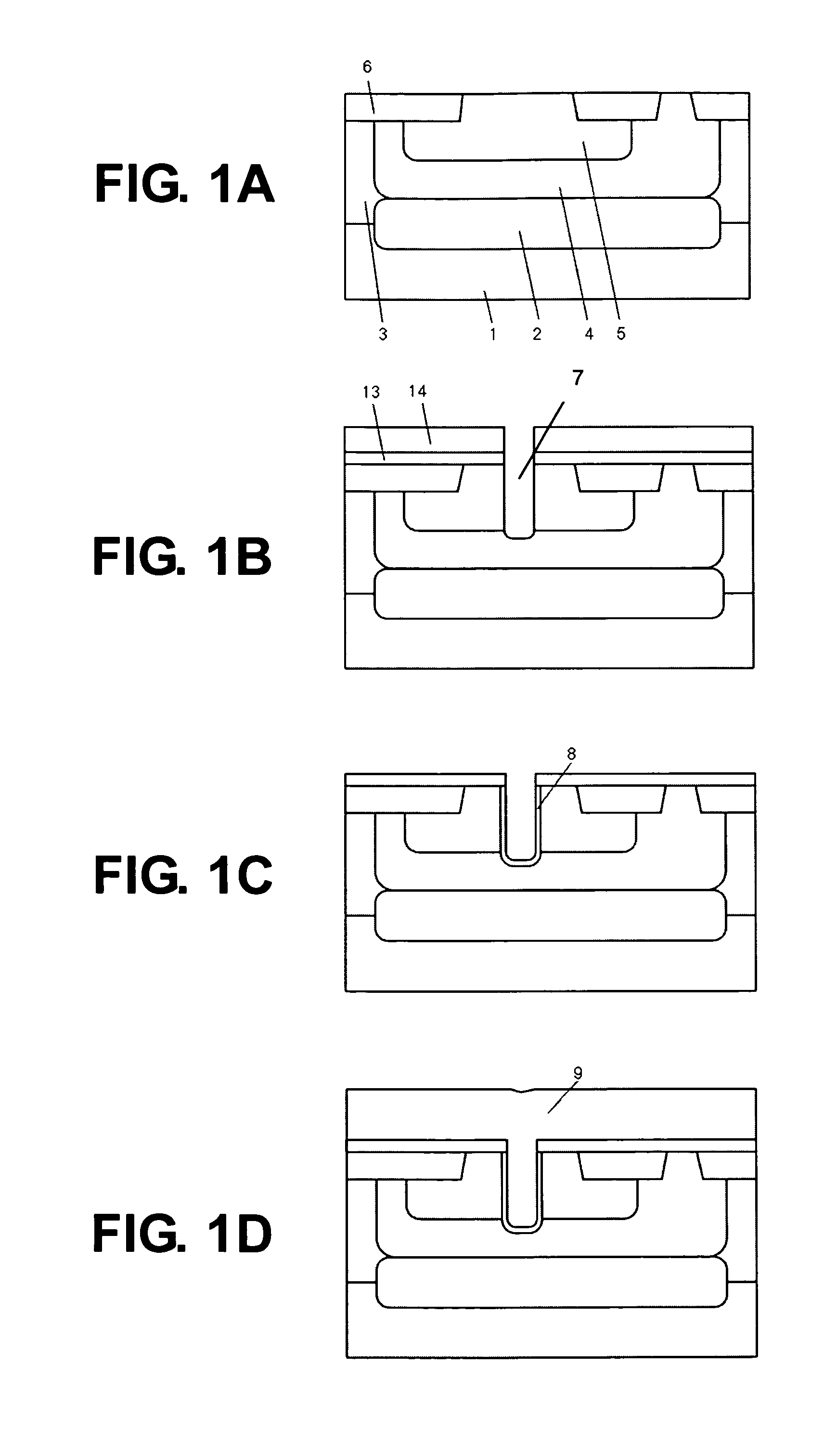
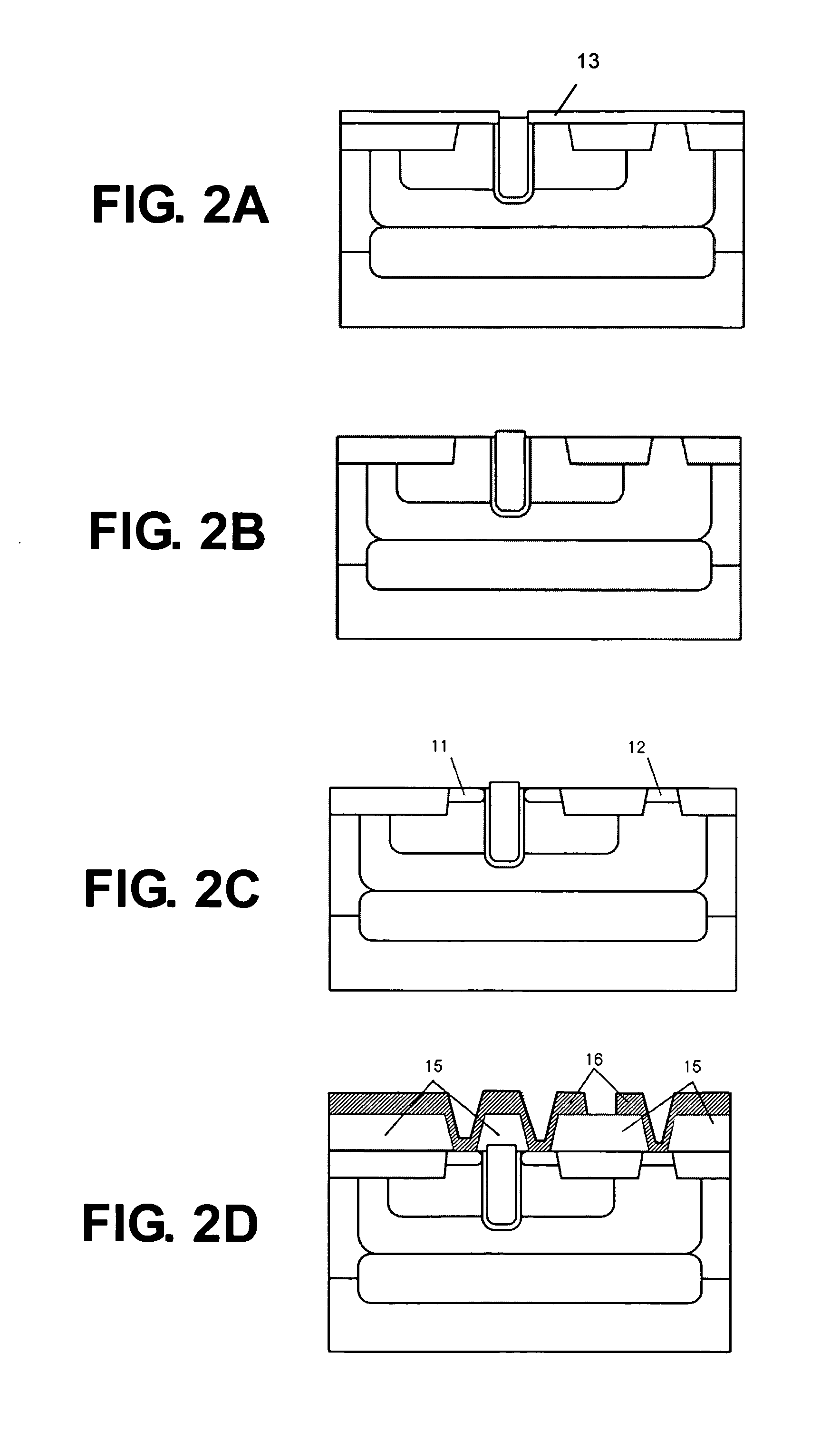
[0020]Hereinafter, a semiconductor device and a method of manufacturing the same according to the present invention are described with reference to the drawings by means of an embodiment. FIGS. 1A to 2D are schematic cross-sectional views illustrating steps of manufacturing the semiconductor device according to the embodiment of the present invention.

[0021]FIG. 1A is a schematic cross-sectional view of the semiconductor device of the present invention, and illustrates a state after the manufacturing steps have been carried out to some extent. On a P type silicon substrate 1, an N+ buried layer 2 is formed, and further on the substrate 1, a P type silicon layer 3 is formed by epitaxial growth. Further, an N− type drain layer 4, which has a concentration lower than that of the N+ buried layer 2, is formed by thermal diffusion and the like, the N− type drain layer 4 being formed so as to reach the N+ buried layer 2 from the surface of the P type silicon layer 3. Further, a P type well ...


PUM


Abstract

Provided is a method of manufacturing a vertical MOSFET having a trench structure, which is capable of performing stable processing. While leaving a silicon nitride film (13) used to form a trench (7) on a surface of a semiconductor substrate, a gate electrode material (9) is buried inside the trench (7), and then the gate electrode material (9) on the silicon nitride film (13) is removed, to thereby form a gate electrode (9) inside the trench (7).

Description

BACKGROUND OF THE INVENTION[0001]1. Field of the Invention[0002]The present invention relates to a method of manufacturing a semiconductor device, and more particularly, to a method of manufacturing a vertical metal oxide silicon field-effect transistor (MOSFET) having a trench structure.[0003]2. Description of the Related Art[0004]Vertical MOSFETs may be classified into a so-called planar type and a so-called trench type. Since low on-resistance characteristic can be easily obtained by its structure of a trench type vertical MOSFET, in which a gate electrode is buried in a trench, practical use is in progress. The structure and manufacturing steps of the vertical MOSFET having such a trench structure are disclosed in, for example, Japanese Published Patent Application No. 2002-359294 and Japanese Published Patent Application No. 11-103052.[0005]Two examples of the structure of the conventional vertical MOSFET are described. In the description below, the symbols −, +, and ++ written...

Claims


Application Information

Patent Timeline
IPC IPC(8): H01L29/78H01L21/336
CPCH01L29/41775H01L29/4236H01L29/7813H01L29/7809H01L29/66734H01L29/66045
Inventor KOBAYASHI, NAOTO
Owner ABLIC INC
Why Eureka
Try Eureka