Small-area and low-voltage Anti-fuse element and array

a low-voltage, array technology, applied in the direction of electrical equipment, semiconductor devices, semiconductor/solid-state device details, etc., can solve the problems of high manufacturing cost, low reliability and high fabrication cost, complex structure of read-only memory and cache memories, etc., to reduce the required puncturing voltage, reduce current, and effectively reduce the area of an element

Active Publication Date: 2022-03-31
YIELD MICROELECTRONICS CORP
View PDF0 Cites 0 Cited by
  • Summary
  • Abstract
  • Description
  • Claims
  • Application Information

AI Technical Summary

Benefits of technology

[0006]Owing to the abovementioned problems, the primary objective of the present invention is to provides a small-area and low-voltage anti-fuse element and an array thereof, wherein an anti-fuse gate overlaps four gate dielectric layers below the gate, whereby the anti-fuse gate are shared by four gate dielectric layers. Further, sharp angles are formed at the corners where the anti-fuse gate overlaps the gate dielectric layers. In operation, the high-density charges at the sharp angles can decrease the required puncturing voltage. Thus, the present invention can greatly reduce the current required to program the anti-fuse elements and effectively decrease the area of an element.

Problems solved by technology

However, these read-only-memory and cache memories have complicated structure, low reliability and high fabrication cost.
After writing, the resistance the fuse increases, and the power consumption rises.
Integrated circuit is developing very fast, and the size thereof is growing smaller and smaller.
The limitation of the technology is that a sufficiently high voltage is needed to induce breakdown of gate dielectric layers.

Method used


Image

  • Small-area and low-voltage Anti-fuse element and array
  • Small-area and low-voltage Anti-fuse element and array
  • Small-area and low-voltage Anti-fuse element and array

Examples


first embodiment

[0020]Refer to FIGS. 1-3 for a

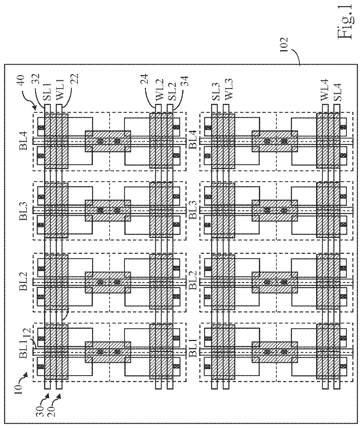
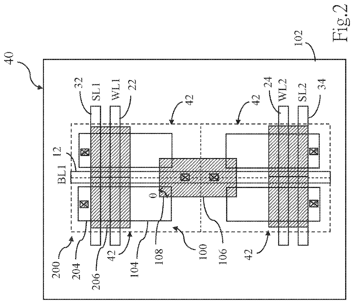
[0021]As shown in FIG. 1, the small-area and low-voltage anti-fuse array of the present invention comprises a plurality of parallel bit lines 10, a plurality of parallel word lines 20, a plurality of parallel select lines 30, and a plurality of anti-fuse element 40. The plurality of bit lines 10 includes bit lines BL1 to BL4, and the bit line BL1 is defined as the first bit line 12. The plurality of word lines 20 is vertical to the bit lines 10 and includes word lines WL1 to WL4, wherein the word lines WL1 and WL2 are defined as the first word line 22 and the second word line 24, which are respectively disposed at two sides of the first bit line 12. The plurality of select lines 30 is parallel to the word lines 20 and includes selection lines SL1 to SL4, wherein the selection line SL1 is defined as the first select line 32 neighboring the first word line 22, and the selection line SL2 is defined as the second select line 34 neighboring the second word l...

second embodiment

[0027]Refer to FIGS. 4-6 for a

[0028]The second embodiment is different from the first embodiment in that each corner of the anti-fuse gate 106 has an extension member 120 in the second embodiment. As shown in FIG. 4, in the second embodiment, the small-area and low-voltage anti-fuse array also comprises a plurality of parallel bit lines 10, a plurality of parallel word lines 20, a plurality of parallel select lines 30, and a plurality of anti-fuse element 40. The plurality of bit lines 10 includes bit lines BL1 to BL4, and the bit line BL1 is defined as the first bit line 12. The plurality of word lines 20 is vertical to the bit lines 10 and includes word lines WL1 to WL4, wherein the word lines WL1 and WL2 are defined as the first word line 22 and the second word line 24, which are respectively disposed at two sides of the first bit line 12. The plurality of select lines 30 is parallel to the word lines 20 and includes selection lines SL1 to SL4, wherein the selection line SL1 is d...


PUM

PropertyMeasurementUnit
sharp angleaaaaaaaaaa
areaaaaaaaaaaa

Abstract

A small-area and low-voltage anti-fuse element comprises four first gate dielectric layers each two symmetrically distributed; and an anti-fuse gate formed on the first gate dielectric layers, wherein four corners of the anti-fuse gate respectively overlap corners of the first gate dielectric layers, which are closest to the anti-fuse gate; each of the four corners of the anti-fuse gate is fabricated to have at least one sharp angle. The present invention is characterized in that four first gate dielectric layers share an anti-fuse gate and that the sharp angle has a higher density of charges. Therefore, the present invention can greatly reduce the size of elements, lower the voltage required to puncture the first gate dielectric layer, and decrease the power consumption. The present invention also discloses a small-area and low-voltage anti-fuse array.

Description

[0001]This application claims priority of Application No. 109133605 filed in Taiwan on 28 Sep. 2020 under 35 U.S.C. § 119; the entire contents of all of which are hereby incorporated by reference.BACKGROUND OF THE INVENTIONField of the Invention[0002]The present invention relates to an anti-fuse element and array, particularly to a small-area and low-voltage anti-fuse element and array.Description of the Prior Art[0003]The data of non-volatile memories, including EEPROM and flash memories, are electrically editable and erasable and will not vanish after power is turned off. Therefore, they are extensively used by information and computer industry. However, these read-only-memory and cache memories have complicated structure, low reliability and high fabrication cost. Therefore, the high-reliability and low-cost one-time programmable (OTP) memories are also often used in many situations. The OTP memories are characterized in using fuses and anti-fuses as elements and having high flex...

Claims


Application Information

Patent Timeline
Patent Type & Authority Applications(United States)
IPC IPC(8): H01L27/112
CPCH01L27/11206H01L23/5252H10B20/20
Inventor HUANG, WEN-CHIENHUANG, YU TINGWU, CHI PEI
Owner YIELD MICROELECTRONICS CORP
Why Eureka
Try Eureka