Semiconductor device, physical quantity sensor, electronic apparatus, and moving object

a technology of electromagnetic field and semiconductor device, applied in the direction of measurement device, electronic circuit testing, instruments, etc., can solve the problems of lack of versatility, significant increase in circuit scale, and disclosure of technique, and achieve high versatility, failure detection rate, and circuit scale increase

Active Publication Date: 2014-10-02
SEIKO EPSON CORP
View PDF18 Cites 1 Cited by
  • Summary
  • Abstract
  • Description
  • Claims
  • Application Information

AI Technical Summary

Benefits of technology

[0007]An advantage of some aspects of the invention is that a semiconductor device, a physical quantity sensor, an electronic apparatus and a moving object in which the failure detection rate can be improved while restraining an increase in circuit scale can be provided by using a technique with high versatility that enables an easier scan test design.

Problems solved by technology

However, this technique leads to a significant increase in circuit scale due to the insertion of a large number of flip-flops.
However, the technique disclosed in JP-A-11-271401 lacks versatility because a flip-flop used as an observation flip-flop is limited to a flip-flop forming a shift register.
Therefore, the scan test design becomes complicated, leading to design errors.
According to the semiconductor device of this application example, since an output signal from the digital circuit to the analog circuit is observable from outside, a failure in the logic circuit (combinational circuit) that generates the output signal.
According to the semiconductor device of this application example, since the propagation to the subsequent circuit of a signal in which the logic level is fixed is stopped at the first selected when in the scan test mode and the second signal is inputted instead of the first signal, a failure in the subsequent circuit can be detected.

Method used


Image

  • Semiconductor device, physical quantity sensor, electronic apparatus, and moving object
  • Semiconductor device, physical quantity sensor, electronic apparatus, and moving object
  • Semiconductor device, physical quantity sensor, electronic apparatus, and moving object

Examples


first embodiment

1-1. First Embodiment

Circuit Configuration

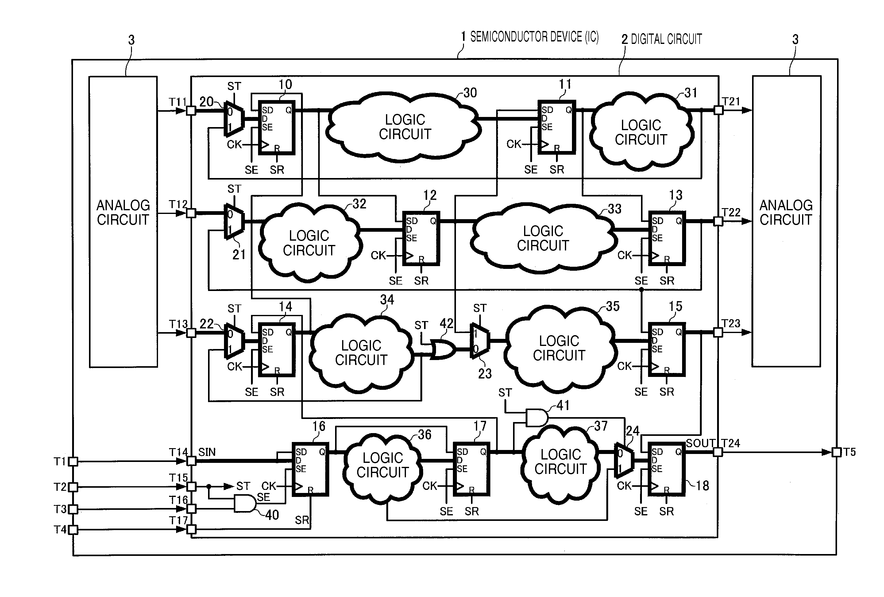
[0050]FIG. 1 shows an example of the configuration of the semiconductor device according to a first embodiment. As shown in FIG. 1, a semiconductor device 1 of the first embodiment includes a digital circuit 2 and analog circuits 3. However, the semiconductor device 1 may not include the analog circuits 3.

[0051]The digital circuit 2 is provided with input terminals T11 to T17 and output terminals T21 to T24.

[0052]A digital signal outputted from the analog circuit 3 (for example, an output signal from an A / D converter) is inputted to the input terminals T11, T12, T13. The input terminals T14, T15, T16, T17 are electrically connected to external input terminals T1, T2, T3, T4 of the semiconductor device 1, respectively. A digital signal inputted from outside the semiconductor device 1 is inputted to the input terminals T14, T15, T16, T17 via the external input terminals T1, T2, T3, T4.

[0053]Digital signals outputted from the output terminals T...

second embodiment

1-2. Second Embodiment

[0103]In the first embodiment, for example, if there are more output signals from the digital circuit 2 to the analog circuit 3 than input signals from the analog circuit 3 to the digital circuit 2, when in the scan test mode, the respective output signals cannot be separately inputted to the selectors provided on the input side of the flip-flops to which the input signals are inputted respectively in the normal operation mode. Thus, in a second embodiment, a multiple-input logic circuit is provided to which plural signals to be monitored when in the scan test mode are inputted, and an output signal from the multiple-input logic circuit is inputted to a selector. The multiple-input logic circuit is provided for the scan test mode and does not function (does not contribute to the operation of the digital circuit 2 in the normal operation mode) when not in the scan test mode (when in the normal operation mode). The input signals to the multiple-input logic circui...


PUM


Abstract

A semiconductor device includes a digital circuit having a scan test mode. The digital circuit includes a first flip-flop forming a part of a scan chain when in the scan test mode, and a first selector provided on an input side of the first flip-flop. The first selector is capable of selecting a first signal when not in the scan test mode, and selecting a second signal that is different from the first signal when in the scan test mode.

Description

BACKGROUND[0001]1. Technical Field[0002]The present invention relates to a semiconductor device, a physical quantity sensor, an electronic apparatus, and a moving object.[0003]2. Related Art[0004]Currently, physical quantity sensors capable of detecting various physical quantities, such as an acceleration sensor that detects acceleration and a gyro sensor that detects angular velocity, are broadly used in various systems and electronic apparatuses. In recent years, very high reliability is required of various physical quantity sensors as these physical sensors are installed on automobiles. To secure high reliability, it is necessary to detect a failure (defect) of a semiconductor device (IC) that processes an output signal from a sensor element, with a probability of almost 100% in the inspection process. As a technique for efficiently detecting a wiring failure (defect) in a digital circuit included in the semiconductor circuit (IC), a scan test is widely known in which flip-flops ...

Claims


Application Information

Patent Timeline
Patent Type & Authority Applications(United States)
IPC IPC(8): G01R31/3177
CPCG01R31/3177G01R31/318558G01R31/318536G01R31/318541G01R31/3167G01R31/31701
Inventor SATO, HIDEKI
Owner SEIKO EPSON CORP
Why Eureka
Try Eureka