Dynamic design attributes for wafer inspection

a technology of dynamic design attributes and wafers, applied in semiconductor/solid-state device testing/measurement, image enhancement, instruments, etc., can solve the problems of affecting the electrical parameters of the device, affecting the performance capability of the process, and small defects, etc., to achieve more sensitive inspections, and reduce the effect of manufacturing processes

Active Publication Date: 2014-10-09
KLA TENCOR TECH CORP
View PDF9 Cites 9 Cited by
  • Summary
  • Abstract
  • Description
  • Claims
  • Application Information

AI Technical Summary

Benefits of technology

[0022]FIG. 5 is a block diagram illustrating one embodiment of a non-transitory computer-readable medium storing program instructions e...

Problems solved by technology

However, as the dimensions of semiconductor devices decrease, inspection becomes even more important to the successful manufacture of acceptable semiconductor devices because smaller defects can cause the devices to fail.
As design rules shrink, however, semiconductor manufacturing processes may be operating closer to the limitations on the performance capability of the processes.
In addition, smaller defects can have an impact on the electrical parameters of the device as the design rules shrink, which drives more sensitive inspections.
Therefore, as design rules shrink, the population of potentially yield relevant defects detected by inspection grows dramatically, and the population of nuisance defects detected by inspection also increases dramatically.
Therefore, more and more defects ...

Method used


Image

  • Dynamic design attributes for wafer inspection
  • Dynamic design attributes for wafer inspection
  • Dynamic design attributes for wafer inspection

Examples


Embodiment Construction

[0025]Turning now to the drawings, it is noted that the figures are not drawn to scale. In particular, the scale of some of the elements of the figures is greatly exaggerated to emphasize characteristics of the elements. It is also noted that the figures are not drawn to the same scale. Elements shown in more than one figure that may be similarly configured have been indicated using the same reference numerals. Unless otherwise noted herein, any of the elements described and shown may include any suitable commercially available elements.

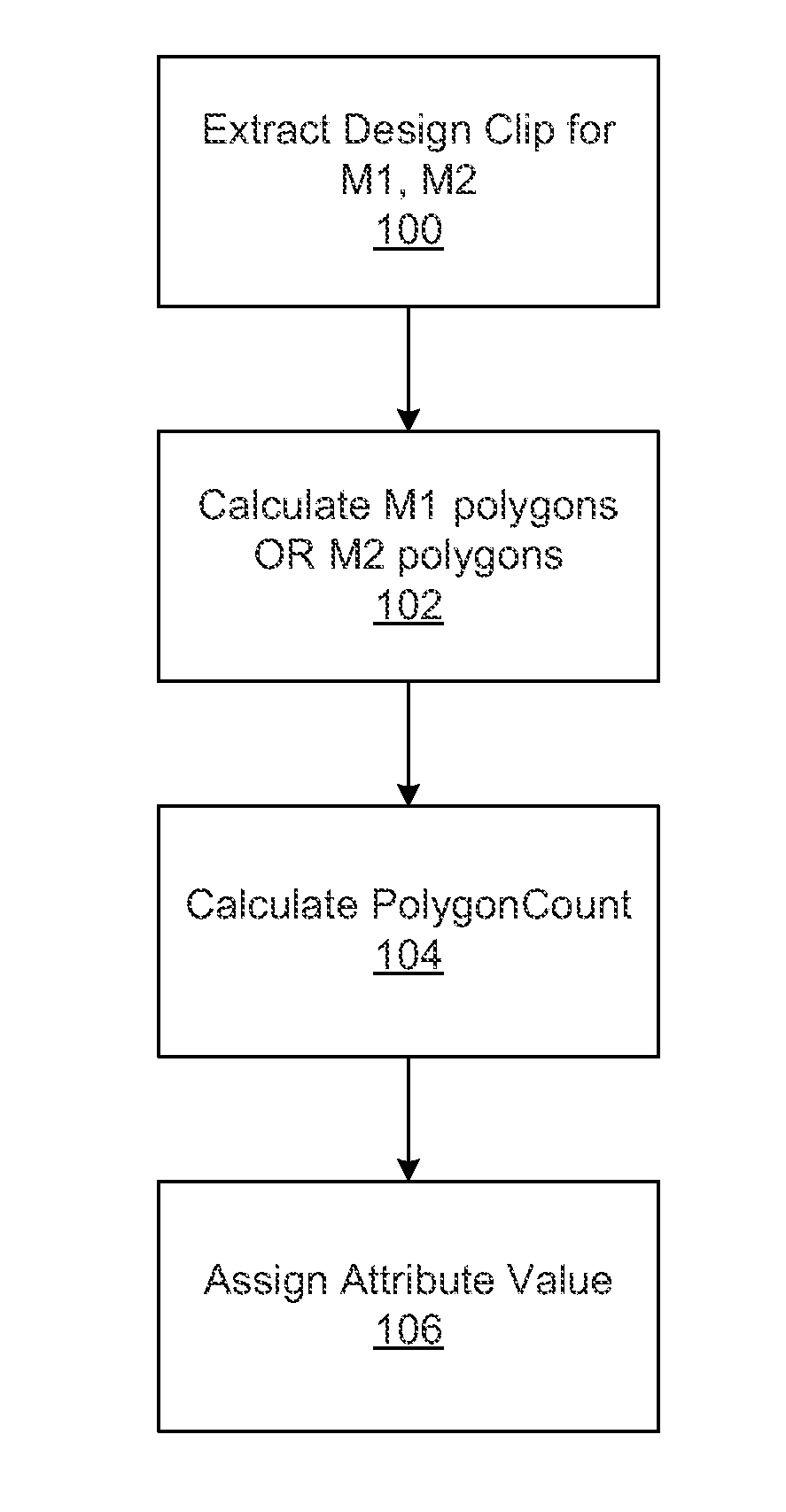
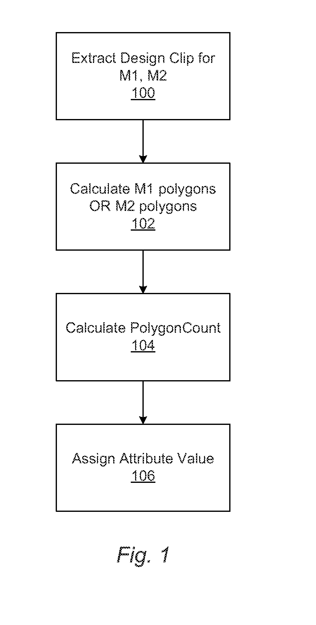
[0026]Design based binning (DBB) is a feature that is part of some wafer inspection tools. This feature enables correlating defect locations based on chip design data. This technology has enabled the following use cases on inspection tools:

[0027]a) Ability to remove systematic nuisance defects;

[0028]b) Systematic defect discovery: and

[0029]c) Systematic defect classification and monitoring.

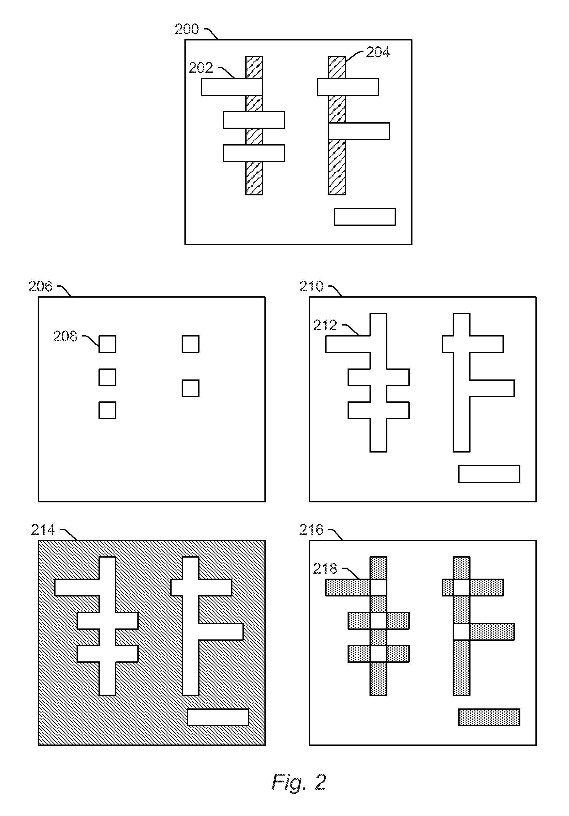
For example, design attributes like pattern density and inter...


PUM


Abstract

Methods and systems for dynamic design attributes for wafer inspection are provided. One method includes, at run time of a wafer inspection recipe, prompting a user of a wafer inspection tool on which the wafer inspection recipe is performed for information for a design based binning (DBB) process. The information includes one or more formulae for calculating design attributes from a design for a wafer. The design attributes are used to bin the defects in the DBB process. The method also includes performing inspection of a wafer according to an updated wafer inspection recipe. Performing the inspection includes binning defects detected on the wafer according to the DBB process in the updated wafer inspection recipe.

Description

BACKGROUND OF THE INVENTION[0001]1. Field of the Invention[0002]This invention generally relates to dynamic design attributes for wafer inspection.[0003]2. Description of the Related Art[0004]The following description and examples are not admitted to be prior art by virtue of their inclusion in this section.[0005]An integrated circuit (IC) design may be developed using a method or system such as electronic design automation (EDA), computer aided design (CAD), and other IC design software. Such methods and systems may be used to generate the circuit pattern database from the IC design. The circuit pattern database includes data representing a plurality of layouts for various layers of the IC. Data in the circuit pattern database may be used to determine layouts for a plurality of reticles. A layout of a reticle generally includes a plurality of polygons that define features in a pattern on the reticle. Each reticle is used to fabricate one of the various layers of the IC. The layers ...

Claims


Application Information

Patent Timeline
IPC IPC(8): G01R31/265
CPCG01R31/2656H01L22/12G01N21/9501G06T7/001G06T2207/30148
Inventor JAYARAMAN, THIRUPURASUNDARIBABULNATH, RAGHAV
Owner KLA TENCOR TECH CORP
Why Eureka
Try Eureka