Semiconductor device and method for manufacturing the same

a semiconductor device and manufacturing method technology, applied in semiconductor devices, diodes, electrical devices, etc., can solve the problems of snapback phenomenon and deterioration of voltage/current characteristics of semiconductor devices, and achieve the suppression of snapback phenomena and deterioration of vi characteristics of semiconductor devices. , the effect of simple manufacturing process

Active Publication Date: 2014-10-16
DENSO CORP
View PDF2 Cites 7 Cited by
  • Summary
  • Abstract
  • Description
  • Claims
  • Application Information

AI Technical Summary

Benefits of technology

[0012]In the above second semiconductor device, the impurity concentration of the first conductivity type impurities and the impurity concentration of the second conductivity type impurities of the cathode layer are both distributed constantly from the lower surface of the semiconductor substrate. Since the impurity concentrations are distributed constantly, by setting the second depth deeper than the first depth, a state in which the impurity concentration of the second condu

Problems solved by technology

In this case, in the cathode layer, if a dose amount of the n-type impurity ions is not high enough to compensate for a dose amount of the p-type imp

Method used


Image

  • Semiconductor device and method for manufacturing the same
  • Semiconductor device and method for manufacturing the same
  • Semiconductor device and method for manufacturing the same

Examples


embodiment 1

[0046](First Semiconductor Device)

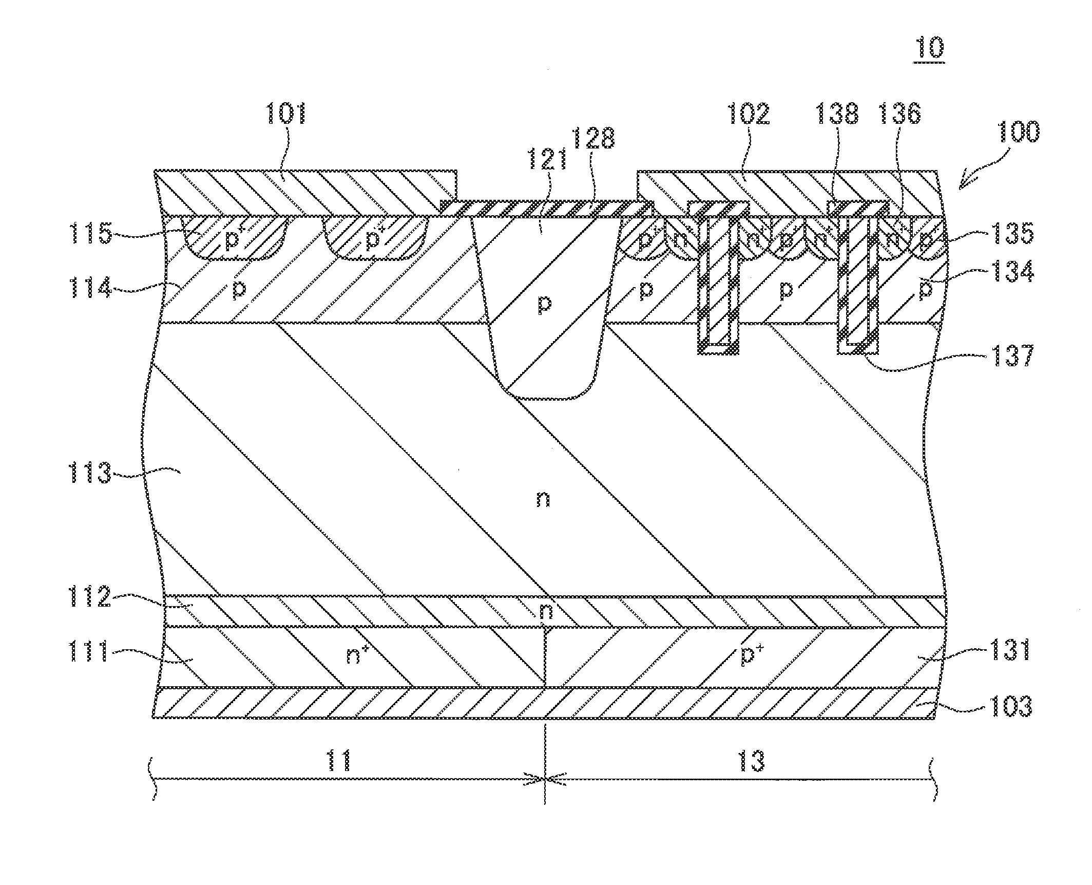
[0047]In an embodiment 1, a first semiconductor device 10 illustrated in FIGS. 1 and 2 is exemplified in explanation. The semiconductor device 10 is an RC-IGBT in which a diode and an IGBT are formed on a semiconductor substrate.

[0048]The semiconductor device 10 comprises a semiconductor substrate 100, an insulated gate 137 formed on an upper surface side of the semiconductor substrate 100 and surface insulating films 128 and 138, upper surface electrodes 101 and 102 in contact with the upper surface of the semiconductor substrate 100, and a lower surface electrode 103 in contact with the lower surface of the semiconductor substrate 100. The semiconductor substrate 100 comprises a diode region 11 and an IGBT region 13. The upper surface electrode 101 is formed on an upper surface of the diode region 11, and the upper surface electrode 102 is formed on an upper surface of the IGBT region 13.

[0049]The semiconductor substrate 100 comprises an n+-type c...

embodiment 2

[0066](Second Semiconductor Device)

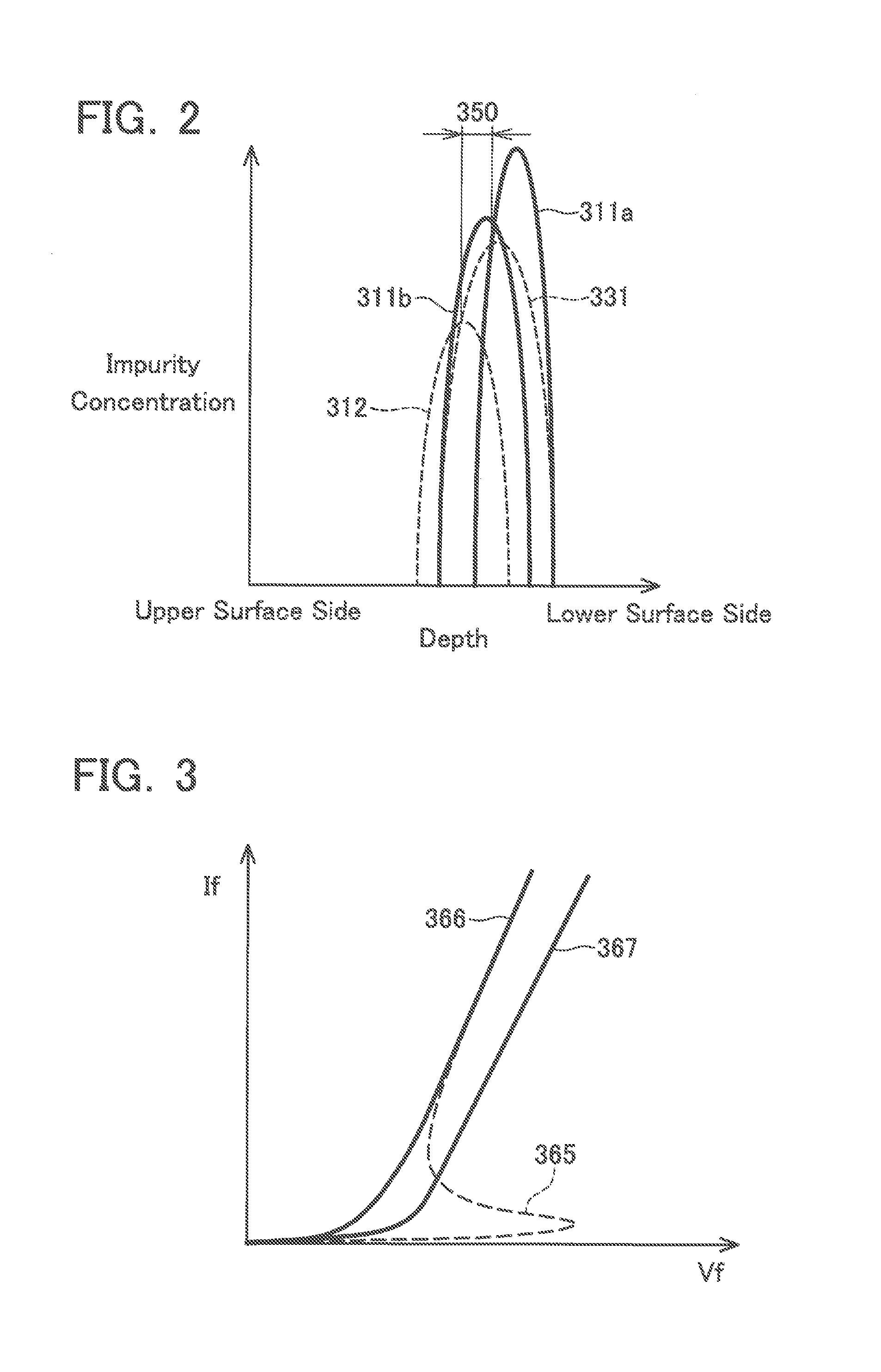
[0067]In an embodiment 2, a semiconductor device 20 illustrated in FIGS. 10 and 11 is exemplified in explanation. Since a section structure of the semiconductor device 20 is similar to the structure of the semiconductor device 10 illustrated in FIG. 1, the explanation will be omitted. The semiconductor device 20 is different from the semiconductor device 10 in the distribution of the impurity concentration in the vicinity of the lower surface of the diode region 11. As illustrated in FIG. 11, in the semiconductor device 20, a distribution 411 of an n-type impurity concentration and a distribution 431 of a p-type impurity concentration of the cathode layer 111 are both distributed constantly to a certain depth from the lower surface of the semiconductor substrate 100. A distribution 412 of the n-type impurity concentration of the buffer layer 112 is distributed in a curve pattern. The distribution 431 has a constant concentration from the lower surf...


PUM


Abstract

A semiconductor device including a semiconductor substrate in which a diode region and an IGBT region are formed is provided. In the semiconductor device, the diode region includes a second conductivity type cathode layer. An impurity concentration of second conductivity type impurities of the cathode layer is distributed in a curve pattern having at least two peaks, and the impurity concentration of the second conductivity type impurities is higher than that of first conductivity type impurities at all depths of the cathode layer.

Description

TECHNICAL FIELD[0001]A technology described in this specification relates to a semiconductor device and a method for manufacturing the same.BACKGROUND ART[0002]A semiconductor device including a semiconductor substrate in which a diode region and an IGBT region are formed has been known. In the diode region, an n-type cathode layer is formed on a lower surface side of the semiconductor substrate, while in the IGBT region, a p-type collector layer is formed on the lower surface side of the semiconductor substrate. The collector layer and the cathode layer are formed in general by doping impurity ions to the lower surface side of the semiconductor substrate. For example, after p-type impurity ions are doped to the entire lower surface of the semiconductor substrate, the region which becomes the collector layer on the lower surface is covered by a mask and n-type impurity ions are doped, and the impurities are diffused by an annealing process. In this case, in the cathode layer, if a d...

Claims


Application Information

Patent Timeline
IPC IPC(8): H01L29/739H01L27/06H01L29/66
CPCH01L29/7395H01L27/0664H01L29/66333H01L21/26513H01L21/268H01L29/0834H01L29/36H01L29/6609H01L29/66348H01L29/7397H01L29/861H01L29/1095
Inventor KAMEYAMA, SATORU
Owner DENSO CORP
Why Eureka
Try Eureka