Semiconductor devices and methods of manufacturing the same

a technology of semiconductor devices and semiconductor layers, which is applied in the direction of semiconductor devices, electrical devices, transistors, etc., can solve the problems of relatively poor gap fill characteristic of the insulation layer formed by the pecvd process, and achieve the effect of reducing the coupling capacitance between the adjacent gate structure, poor gap fill characteristic, and large width

Inactive Publication Date: 2014-10-16
SAMSUNG ELECTRONICS CO LTD
View PDF7 Cites 2 Cited by
  • Summary
  • Abstract
  • Description
  • Claims
  • Application Information

AI Technical Summary

Benefits of technology

[0029]According to example embodiments, an insulation layer may be formed by a PECVD process using SiH4 gas as a source gas and N2O gas as an oxidation gas at a relative low pressure. The insulation layer formed by the PECVD process may have a relatively poor gap fill characteristic. Thus, an air gap having a relatively large width may be formed in the insulation layer. Accordingly, a coupling capacitance between the adjacent gate structures may decrease.

Problems solved by technology

The insulation layer formed by the PECVD process may have a relatively poor gap fill characteristic.

Method used


Image

  • Semiconductor devices and methods of manufacturing the same
  • Semiconductor devices and methods of manufacturing the same
  • Semiconductor devices and methods of manufacturing the same

Examples


Embodiment Construction

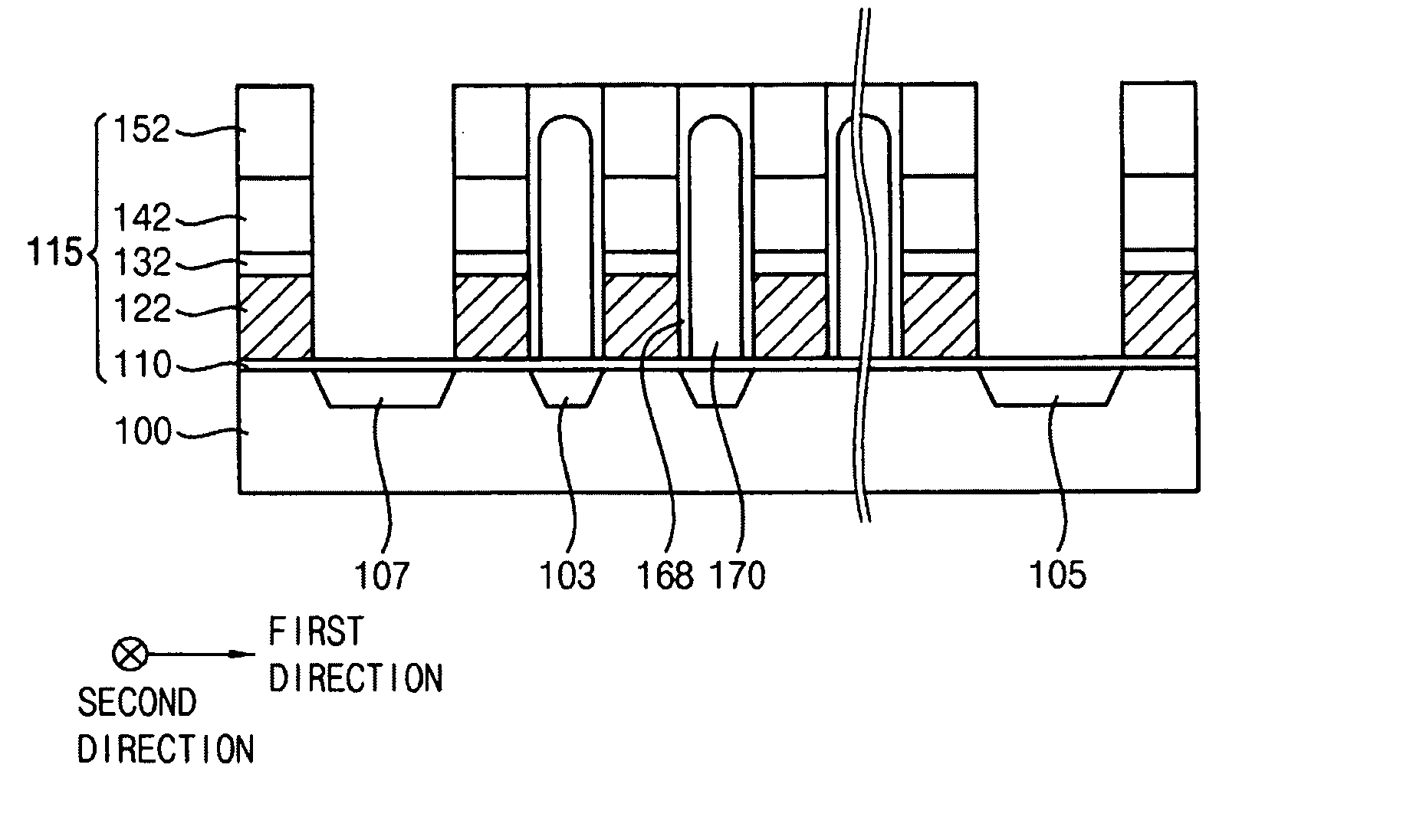
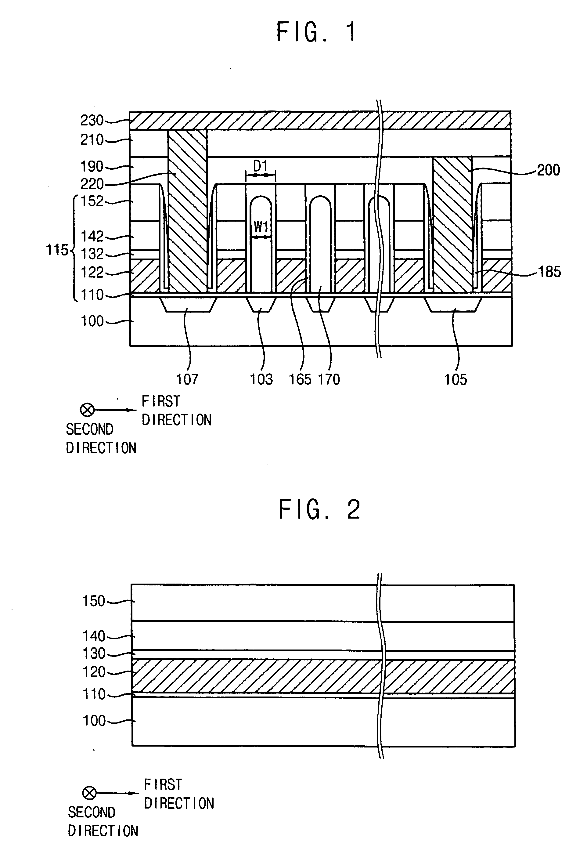
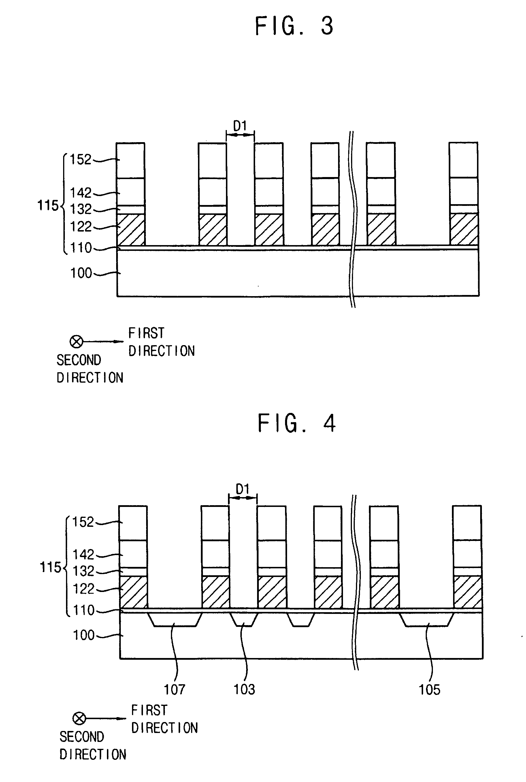
[0037]Various example embodiments will be described more fully hereinafter with reference to the accompanying drawings, in which some example embodiments are shown. The present inventive concepts may, however, be embodied in many different forms and should not be construed as limited to the example embodiments set forth herein. Rather, these example embodiments are provided so that this description will be thorough and complete, and will fully convey the scope of the present inventive concepts to those skilled in the art. In the drawings, the sizes and relative sizes of layers and regions may be exaggerated for clarity.

[0038]It will be understood that when an element or layer is referred to as being “on,”“connected to” or “coupled to” another element or layer, it can be directly on, connected or coupled to the other element or layer or intervening elements or layers may be present. In contrast, when an element is referred to as being “directly on,”“directly connected to” or “directl...


PUM


Abstract

In the method, a plurality of gate structures may be formed on a substrate and be spaced apart from each other in a first direction. An insulation layer pattern may be formed by performing a chemical vapor deposition process using SiH4 gas as a source gas. The insulation layer pattern may partially define an air gap between the adjacent gate structures. A width of the air gap in the first direction may be about 65% to about 70% of a distance between the adjacent gate structures.

Description

CLAIM OF PRIORITY[0001]This application claims priority under 35 USC §119 to Korean Patent Application No. 2013-0039712, filed on Apr. 11, 2013 in the Korean Intellectual Property Office (KIPO), the contents of which are herein incorporated by reference in their entirety.BACKGROUND[0002]1. Field[0003]Example embodiments relate to semiconductor devices and / or methods of manufacturing semiconductor devices. Particularly, example embodiments relate to semiconductor device having air gaps and / or methods of manufacturing the same.[0004]2. Description of the Related Art[0005]Recently, as semiconductor devices are highly integrated, a distance between gate structures or word lines also decreases. Therefore, a parasitic capacitance or a cell coupling between the gate structures or the word lines occurs, thus changing a threshold voltage of the gate structure.[0006]Therefore, semiconductor devices that prevent or reduce the parasitic capacitance or the cell coupling are being studied.SUMMARY...

Claims


Application Information

Patent Timeline
Patent Type & Authority Applications(United States)
IPC IPC(8): H01L29/423H01L21/28
CPCH01L21/28273H01L29/42324H01L21/764H01L29/7881H10B41/30H01L21/02274H01L21/76801H01L21/76829H10B41/00
Inventor LEE, JE-DONGKIM, YOUNG-ILKIM, IL-WOOLEE, KWANG-JAEJEON, IN-HWAHWANG, SUNG-JOON
Owner SAMSUNG ELECTRONICS CO LTD
Why Eureka
Try Eureka