
Multijunction photovoltaic device having sige(SN) and gaasnsb cells

a photovoltaic device and multi-junction technology, applied in photovoltaic energy generation, electrical equipment, climate sustainability, etc., can solve the problems of limited pattern matching and introduce defects into the structure, and achieve good absorption coverage of the spectral wavelengths longer, small band gap, and high absorption efficiency

Inactive Publication Date: 2014-11-27
IQE
View PDF5 Cites 3 Cited by
  • Summary
  • Abstract
  • Description
  • Claims
  • Application Information

AI Technical Summary

Benefits of technology

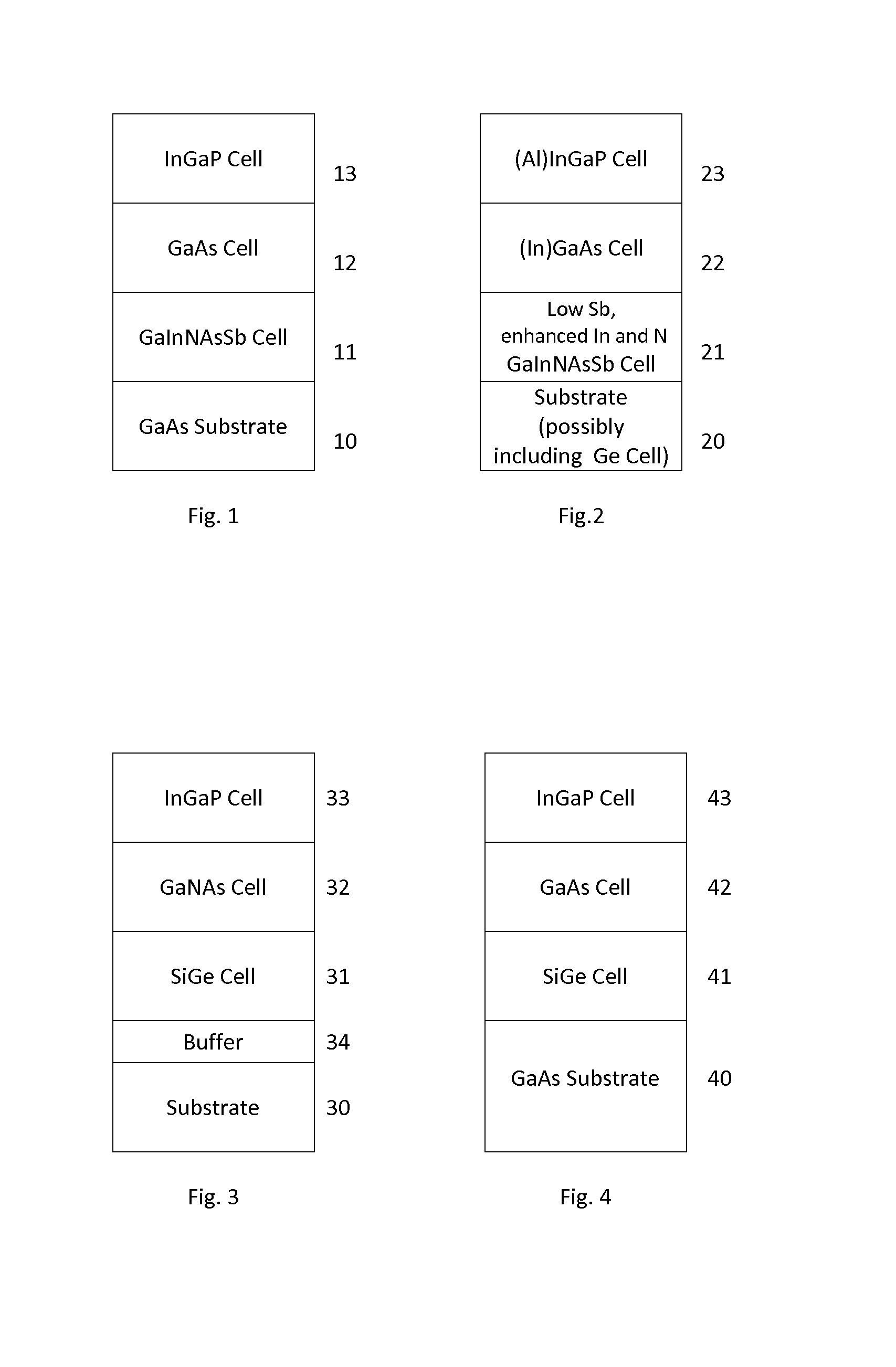
[0034]The gallium nitride arsenide antimonide subcell and silicon germanium, or silicon germanium tin, subcell of the invention are able between them to provide good absorption coverage of the spectral wavelengths longer than those absorbed by, for example, a gallium arsenide subcell, offering high absorption efficiency. This is in contrast of the approach of US2009 / 00140161 (FIG. 1) and US2011 / 0232730 (FIG. 2) which have only one such subcell, and in those the subcell is of a different and more complex material, namely GaInNAsSb. Further, the former document explicitly states that the goal is to have as small a bandgap as possible for the GaInNAsSb. Also, in US2011 / 0083729 (FIG. 3) there are GaNAs and SiGe layers that absorb in this general area of the spectrum but GaNAs cannot be lattice matched to GaAs which means that in that device a strain relieving buffer layer has to be used between its subcells and the substrate. Further this device has no subcell in the 1.4 eV region that would be provided by GaAs, and none could be provided simply because it would not lattice match the GaNAs—further, the InGaP subcell in this device would in order to lattice match GaNAs have a larger bandgap (by changing the proportion of In and Ga) than the InGaP subcell used in the examples of the present invention which is lattice matched to GaAs, leaving a large gap in the absorption spectrum of the device of US2011 / 0083729.

Problems solved by technology

The document notes a problem with Ge bottom subcells, which is that because of the small bandgap the current produced by Ge subcells is high compared to GaAs and InGaP top and middle subcells leading to inefficiency.
In this device the lattice matching is limited.
This is produced by changing the composition of the buffer layer while it is grown to change the lattice parameter, which is not only a complex operation but will introduce defects into the structure.

Method used


Image

  • Multijunction photovoltaic device having sige(SN) and gaasnsb cells
  • Multijunction photovoltaic device having sige(SN) and gaasnsb cells
  • Multijunction photovoltaic device having sige(SN) and gaasnsb cells

Examples


Embodiment Construction

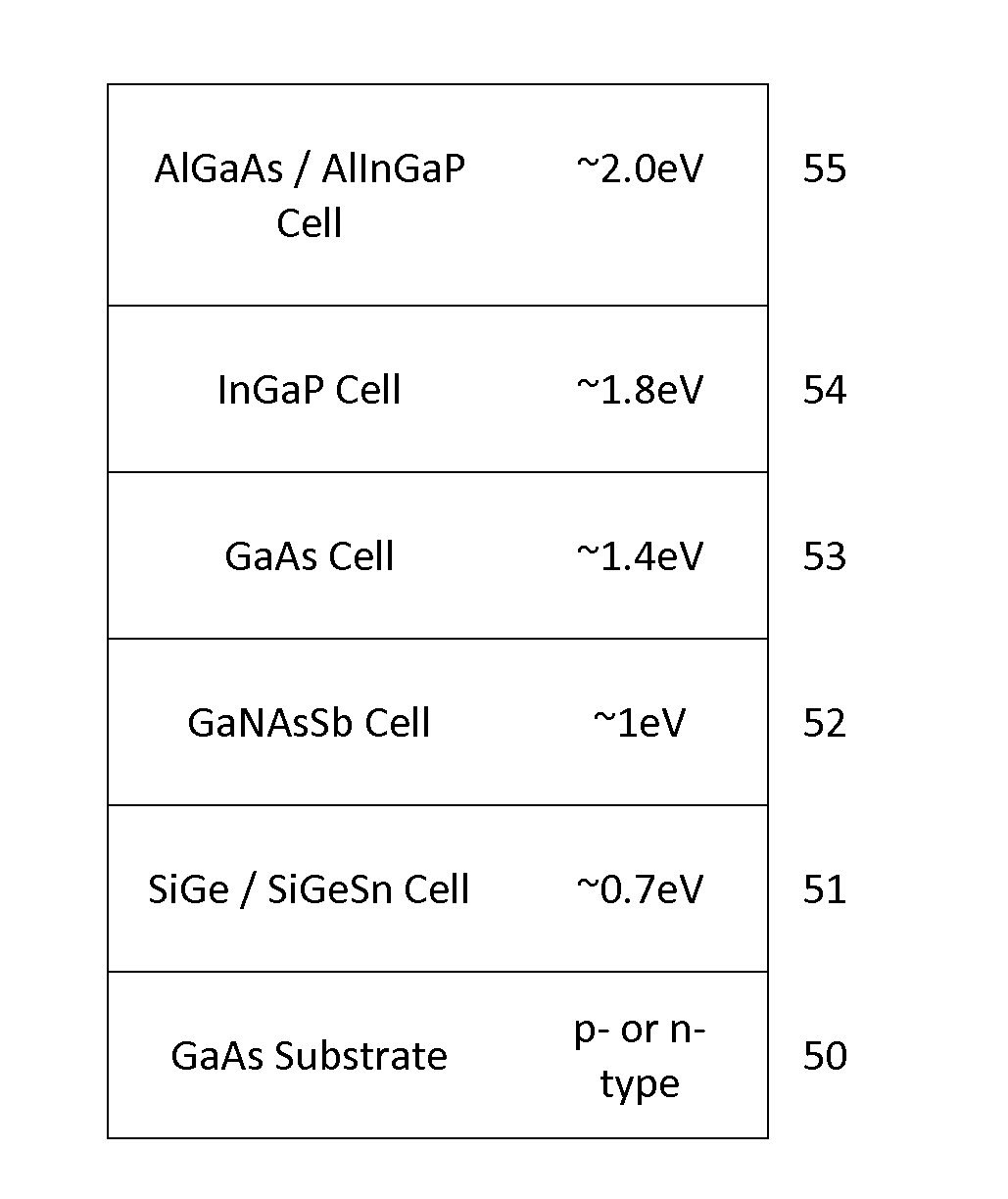
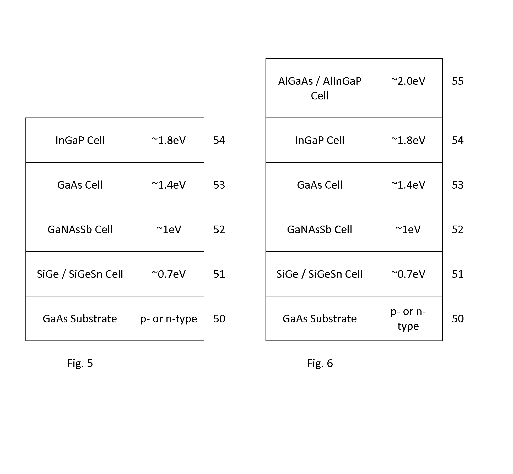
[0045]FIG. 5 shows the subcells of first example of a multijunction photovoltaic device, in particular a solar cell, in accordance with the invention. This comprises a series of subcells to absorb incident light, formed on a GaAs substrate 50. The light is first incident on the subcell 54, which in this example is furthest from the substrate, with light not absorbed by each subcell passing to the next. In this example there are a top subcell 54 comprising a light absorbing layer of InGaP material, an upper middle subcell 53 comprising a light absorbing layer of GaAs 52 and a lower middle subcell comprising a light absorbing layer of GaNAsSb material and a bottom subcell 51 comprising a light absorbing layer of SiGe material, all of which are lattice matched to a GaAs substrate 50. The light absorbing material layer of each of these subcells contains a p-n junction to separate the photocarriers generated. Preferably the cells are connected in series (tandem cell).

[0046]In this exampl...


PUM

PropertyMeasurementUnit
lattice matchedaaaaaaaaaa
latticeaaaaaaaaaa
spectrumaaaaaaaaaa

Abstract

A multijunction tandem photovoltaic device is disclosed having a bottom subcell of silicon germanium or silicon germanium tin material and above that a subcell of gallium nitride arsenide antimonide material. The materials are lattice matched to gallium arsenide, which preferably forms the substrate. Preferably, further lattice matched subcells of gallium arsenide, indium gallium phosphide and aluminium gallium arsenide or aluminium indium gallium phosphide are provided.

Description

[0001]The present invention relates to photovoltaic devices having more than one subcell for absorbing different parts of the spectrum of the incident light.BACKGROUND[0002]Multijunction photovoltaic devices comprise a series of subcells each having a light absorbing semiconductor material and a p-n junction therein to separate the photocarriers, to produce the photocurrent. They work by having a top subcell, i.e. that first exposed to the incident light, that has a large bandgap and so absorbs the shorter wavelengths in the incident light only and passes the longer wavelengths, with the next subcell having a smaller bandgap so that it can absorb part of the light passed by the subcell above, and so on. Solar cells are, of course, one kind of photovoltaic device and are ones used to convert sunlight into electricity for the purpose of generating power.[0003]In this document “top” and “bottom” are to be understood in that sense, i.e. the top subcell is that which receives the inciden...

Claims


Application Information

Patent Timeline
Patent Type & Authority Applications(United States)
IPC IPC(8): H01L31/0725H01L31/0216H01L31/18H01L31/0735H01L31/074
CPCH01L31/0725H01L31/0735H01L31/02167H01L31/1812H01L31/1844H01L31/074H01L31/03044H01L31/0687H01L31/06875Y02E10/544Y02E10/547Y02P70/50H01L29/16H01L29/20H01L29/267H01L31/0328H01L31/068
Inventor JOHNSON, ANDREW
Owner IQE
Learn More