Directed epitaxial heterojunction bipolar transistor
a bipolar transistor and heterojunction technology, applied in transistors, semiconductor devices, electrical equipment, etc., to achieve the effect of reducing the discontinuity between the base-emitter junction and/or the collector junction of the base-emitter junction
- Summary
- Abstract
- Description
- Claims
- Application Information
AI Technical Summary
Benefits of technology
Problems solved by technology
Method used
Image
Examples
first embodiment
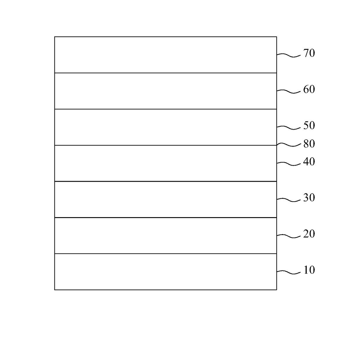
[0021]FIG. 1 is a sectional view showing a directed epitaxial heterojunction bipolar transistor (HBT) structure according to the present invention. As shown in FIG. 1, the directed epitaxial HBT of the present invention includes a sub-collector layer 20, a collector layer 30, a base layer 40, an emitter layer 50, an emitter cap layer 60 and an ohmic contact layer 70, which are sequentially stacked on the substrate 10. Specifically, the sub-collector layer 20 is formed by N-type group III-V semiconductors, and stacked on the substrate 10. The substrate 10 is preferably formed by GaAs that is formed by a (100) face towards a (111)B face with an angle of inclination between 0.6° and 25°. Moreover, the collector layer 30 is stacked on the sub-collector layer 20 and formed by N-type group III-V semiconductors. The base layer 40 is stacked on the collector layer 30 and formed by P-type group III-V semiconductors. The emitter layer 50 is stacked on the base layer 40 and is formed by N-type...
second embodiment
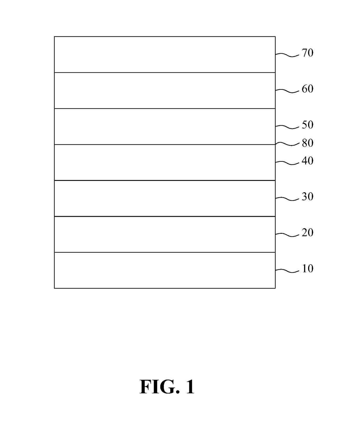
[0025]FIG. 2 is a sectional view showing the directed epitaxial HBT structure according to the present invention. The directed epitaxial HBT of the present invention includes a sub-collector layer 20, a collector layer 30, a tunnel collector layer 35, a base layer 40, an emitter layer 50, an emitter cap layer 60 and an ohmic contact layer 70, which are sequentially stacked on the substrate 10. Similarly, the sub-collector layer 20 is formed by N-type group III-V semiconductors, and is stacked on the substrate 10. The substrate 10 is formed by GaAs that is formed by a (100) face towards a (111)B face with an angle of inclination between 0.6° and 25°.
[0026]It should be noted that the second embodiment shown in FIG. 2 is similar to the first embodiment of FIG. 1, and the primary difference between the first embodiment and the second embodiment is that the second embodiment further includes the tunnel collector layer 35 formed by InGaP or InGaAsP and provided between the collector layer...
third embodiment
[0027]FIG. 3 is a sectional view showing the directed epitaxial HBT structure according to the present invention. As shown in FIG. 3, the directed epitaxial HBT of the present invention includes an intermediate composite layer 15, a sub-collector layer 20, a collector layer 30, a base layer 40, an emitter layer 50, an emitter cap layer 60 and an ohmic contact layer 70, which are sequentially stacked on the substrate 10. The intermediate composite layer 15 is formed by semiconductor materials and is stacked on the substrate 10. Accordingly, the substrate 10 is formed by GaAs that is formed by a (100) face towards a (111)B face with an angle of inclination between 0.6° and 25°.
[0028]It should be noted that the third embodiment shown in FIG. 3 is similar to the first embodiment shown in FIG. 1. The primary difference between the first embodiment and the third embodiment is that the third embodiment further includes the intermediate composite layer 15 which is provided between the subst...
PUM
 Abstract
Description
Claims
Application Information


