
Limited maximum fields of electrode-switching layer interfaces in Re-RAM cells

a re-ram cell, electrode-switching layer technology, applied in the direction of bulk negative resistance effect devices, electrical equipment, semiconductor devices, etc., can solve the problems of affecting the endurance affecting the yield affecting the performance of the re-ram cell, so as to achieve low work functions, high dielectric permittivities, and high electron affinities

Inactive Publication Date: 2014-10-14
SANDISK TECH LLC +2
View PDF21 Cites 2 Cited by
  • Summary
  • Abstract
  • Description
  • Claims
  • Application Information

AI Technical Summary

Benefits of technology

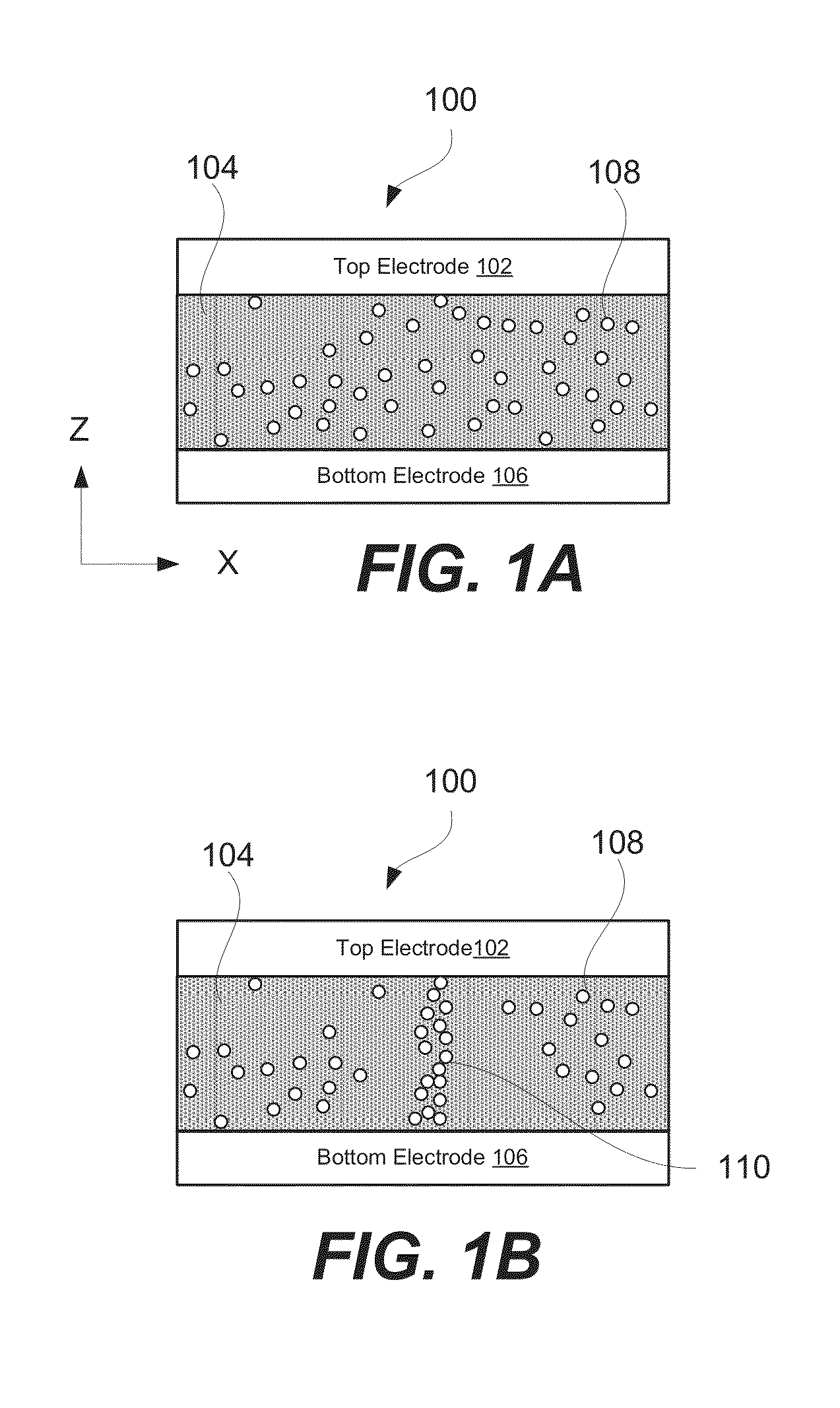
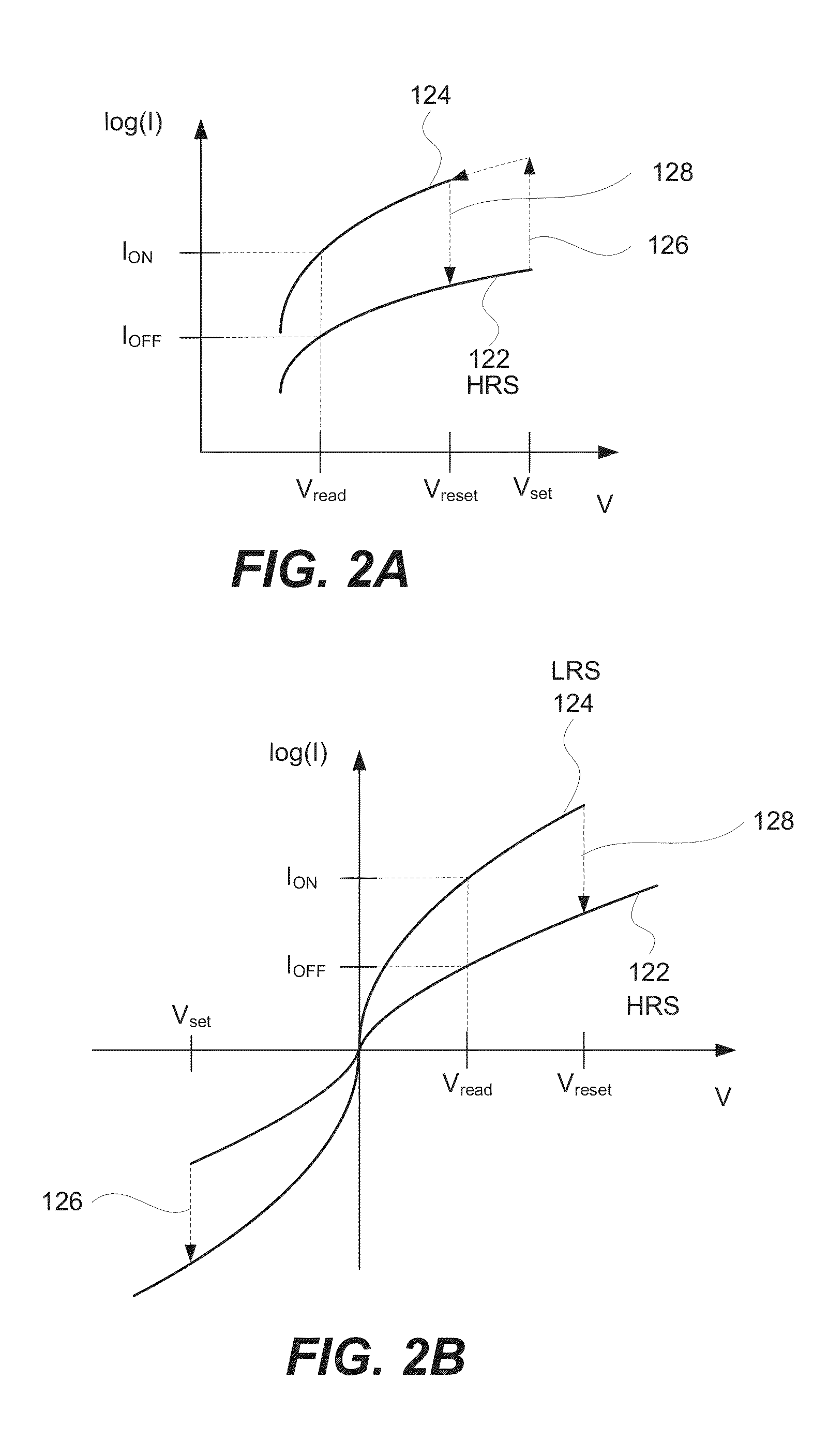
This patent describes a type of material used in a type of memory called ReRAM. The material has a very strong interface between a metal electrode and a layer of resistive switching material. The electrode materials have low work functions, while the resistive switching materials have high dielectric permittivities and electron affinities. The resistive switching material can be niobium oxide. The first layer is made of doped tantalum nitride, while the second layer is made of a resistive switching material. The doped tantalum nitride has a low work function and the resistive switching material has a high work function. The resistive random access memory cell has three layers - a first layer, a second layer, and a third layer. The first and second layers have interfaces, while the third layer has a single interface. The thickness of the layers is between 5 Angstroms and 1,000 Angstroms. The technical effects of this patented material are improved performance and reliability of the ReRAM memory.

Problems solved by technology

As such, the performance of the ReRAM cell may degrade as the concentration and location of the defects in the resistive switching layer change overtime during operation of the ReRAM cell.
For example, a large built-in voltage can cause injection of positive ions (e.g., metal ions) into a resistive switching layer, which may impact its endurance.
It has been found that large built-in voltages can negatively impact yields.
However, conventionally used platinum electrodes may have too large of a work function (in comparison to the proposed electrodes) and may not be suitable for the proposed ReRAM cells.
In this case, a resistance switching layer with very low levels (e.g., 100-30 kOhm) of resistance in the LRS may be limited in terms of scaling down.

Method used


Image

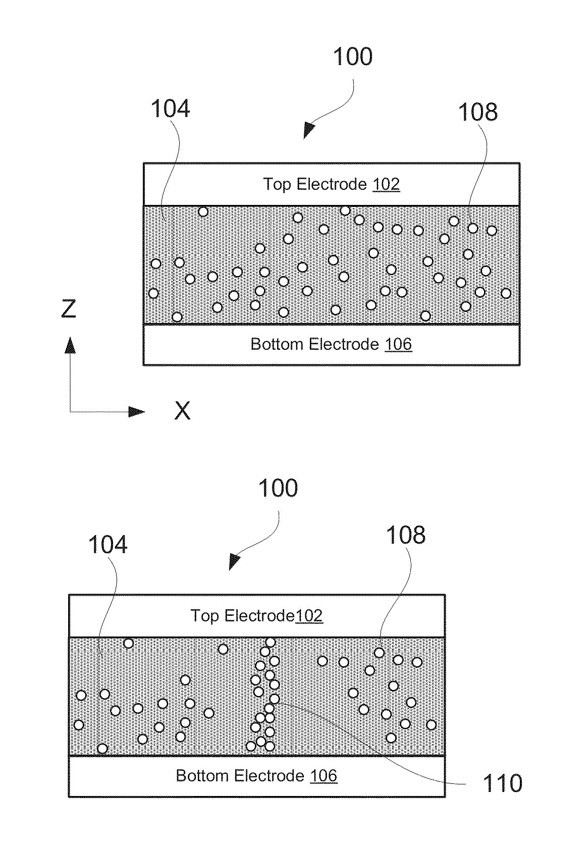
  • Limited maximum fields of electrode-switching layer interfaces in Re-RAM cells
  • Limited maximum fields of electrode-switching layer interfaces in Re-RAM cells
  • Limited maximum fields of electrode-switching layer interfaces in Re-RAM cells

Examples


Embodiment Construction

[0017]A detailed description of various embodiments is provided below along with accompanying figures. The detailed description is provided in connection with such embodiments, but is not limited to any particular example. The scope is limited only by the claims and numerous alternatives, modifications, and equivalents are encompassed. Numerous specific details are set forth in the following description in order to provide a thorough understanding. These details are provided for the purpose of example and the described techniques may be practiced according to the claims without some or all of these specific details. For the purpose of clarity, technical material that is known in the technical fields related to the embodiments has not been described in detail to avoid unnecessarily obscuring the description.

INTRODUCTION

[0018]A ReRAM cell exhibiting resistive switching characteristics generally includes multiple layers formed into a stack. This stack is sometimes referred to as a Meta...


PUM

PropertyMeasurementUnit
work functionaaaaaaaaaa

Abstract

Provided are ReRAM cells, each having at least one interface between an electrode and a resistive switching layers with a maximum field value of less than 0.25. The electrode materials forming such interfaces include tantalum nitrides doped with lanthanum, aluminum, erbium yttrium, or terbium (e.g., TaX(Dopant)YN, where X is at least about 0.95). The electrode materials have low work functions (e.g., less than about 4.5 eV). At the same time, the resistive switching materials have high relative dielectric permittivities (e.g., greater than about 30) and high electron affinities (greater than about for 3.5 eV). Niobium oxide is one example of a suitable resistive switching material. Another electrode interfacing the resistive switching layer may have different characteristics and, in some embodiments, may be an inert electrode.

Description

TECHNICAL FIELD[0001]The present invention relates generally to non-volatile memory and more specifically to resistive random access memory (ReRAM) cells having interfaces between their electrodes and resistive switching layers that have limited maximum fields.BACKGROUND[0002]Nonvolatile memory is computer memory capable of retaining the stored information even when unpowered. Non-volatile memory is typically used for the task of secondary storage or long-term persistent storage and may be used in addition to volatile memory, which losses the stored information when unpowered. Nonvolatile memory can be permanently integrated into computer systems (e.g., solid state hard drives) or can take the form of removable and easily transportable memory cards (e.g., USB flash drives). Nonvolatile memory is becoming more popular because of its small size / high density, low power consumption, fast read and write rates, retention, and other characteristics.[0003]Flash memory is a common type of no...

Claims


Application Information

Patent Timeline
Patent Type & Authority Patents(United States)
IPC IPC(8): H01L45/00
CPCH01L45/1253H01L45/1608H01L45/08H01L27/2463H01L45/146H10B63/80H10N70/24H10N70/841H10N70/8833H10N70/023H10N70/026
Inventor TENDULKAR, MIHIRHASHIM, IMRANMINVIELLE, TIMWANG, YUNYAMAGUCHI, TAKESHI
Owner SANDISK TECH LLC
Learn More