Organic light emitting display apparatus and method of manufacturing the same

Active Publication Date: 2014-11-27
SAMSUNG DISPLAY CO LTD
View PDF12 Cites 57 Cited by
  • Summary
  • Abstract
  • Description
  • Claims
  • Application Information

AI Technical Summary

Benefits of technology

[0006]The present invention provides an organic light emitting display apparatus conducive for a process of mass-producing

Problems solved by technology

Particularly, in medium-large sized top emission type organic light emitting display apparatuses, voltage d

Method used


Image

  • Organic light emitting display apparatus and method of manufacturing the same
  • Organic light emitting display apparatus and method of manufacturing the same
  • Organic light emitting display apparatus and method of manufacturing the same

Examples


Embodiment Construction

[0036]Since the present invention may have various modifications and several embodiments, exemplary embodiments are shown in the drawings and will be described in detail. However, is the invention is not to be limited to the exemplary embodiments set forth herein but rather, the invention should be understood as including all modifications, equivalents, and substitutes.

[0037]Hereinafter, the exemplary embodiments of the present invention will be described in detail with reference to the attached drawings.

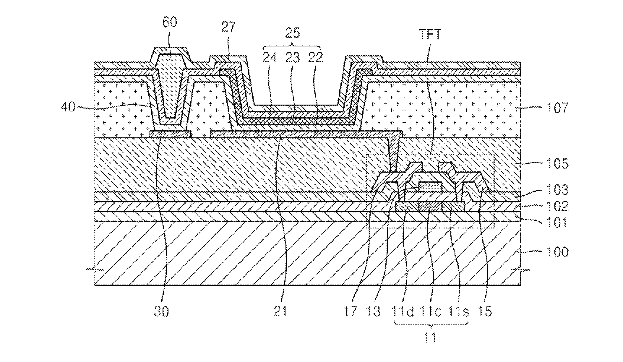
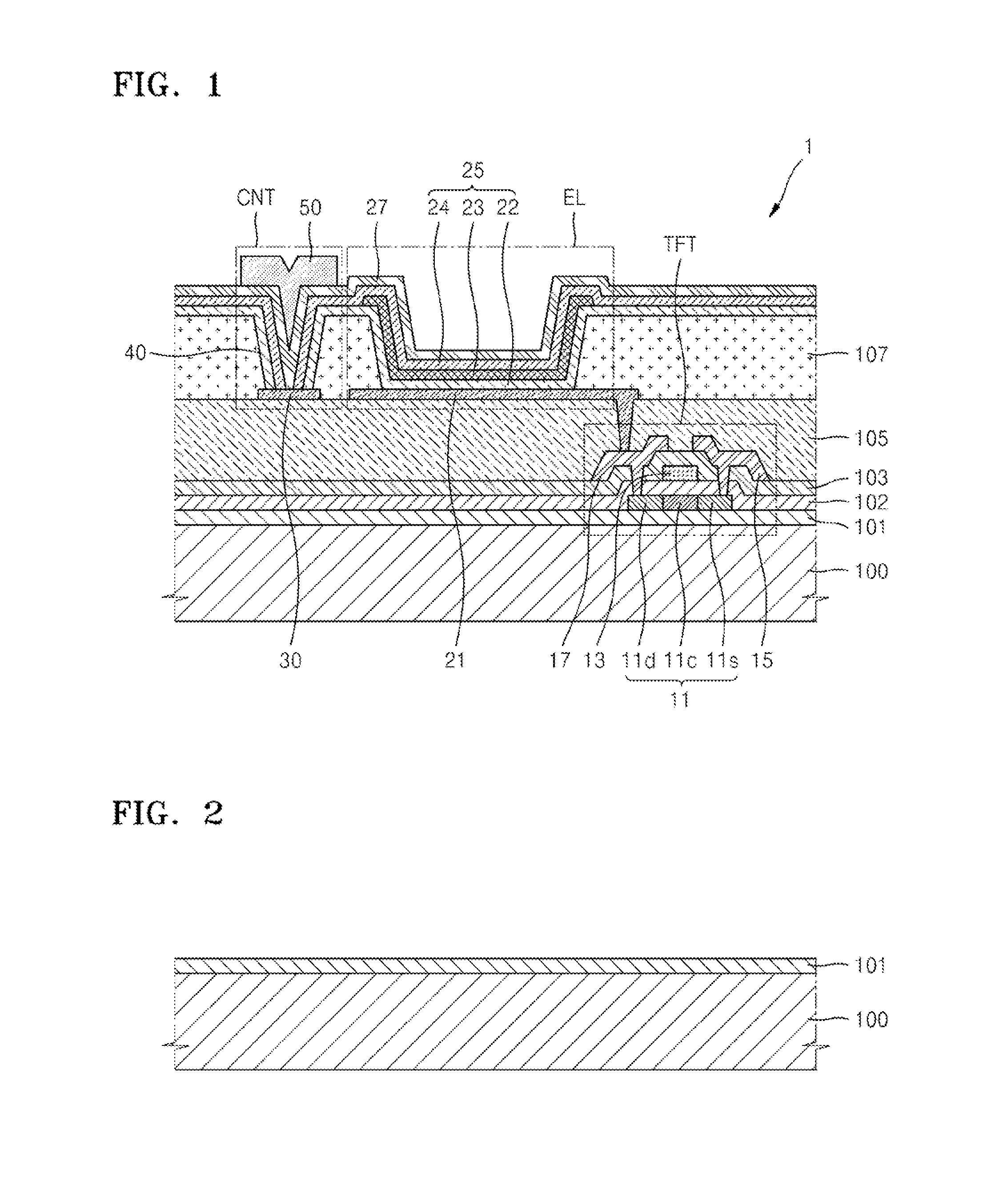
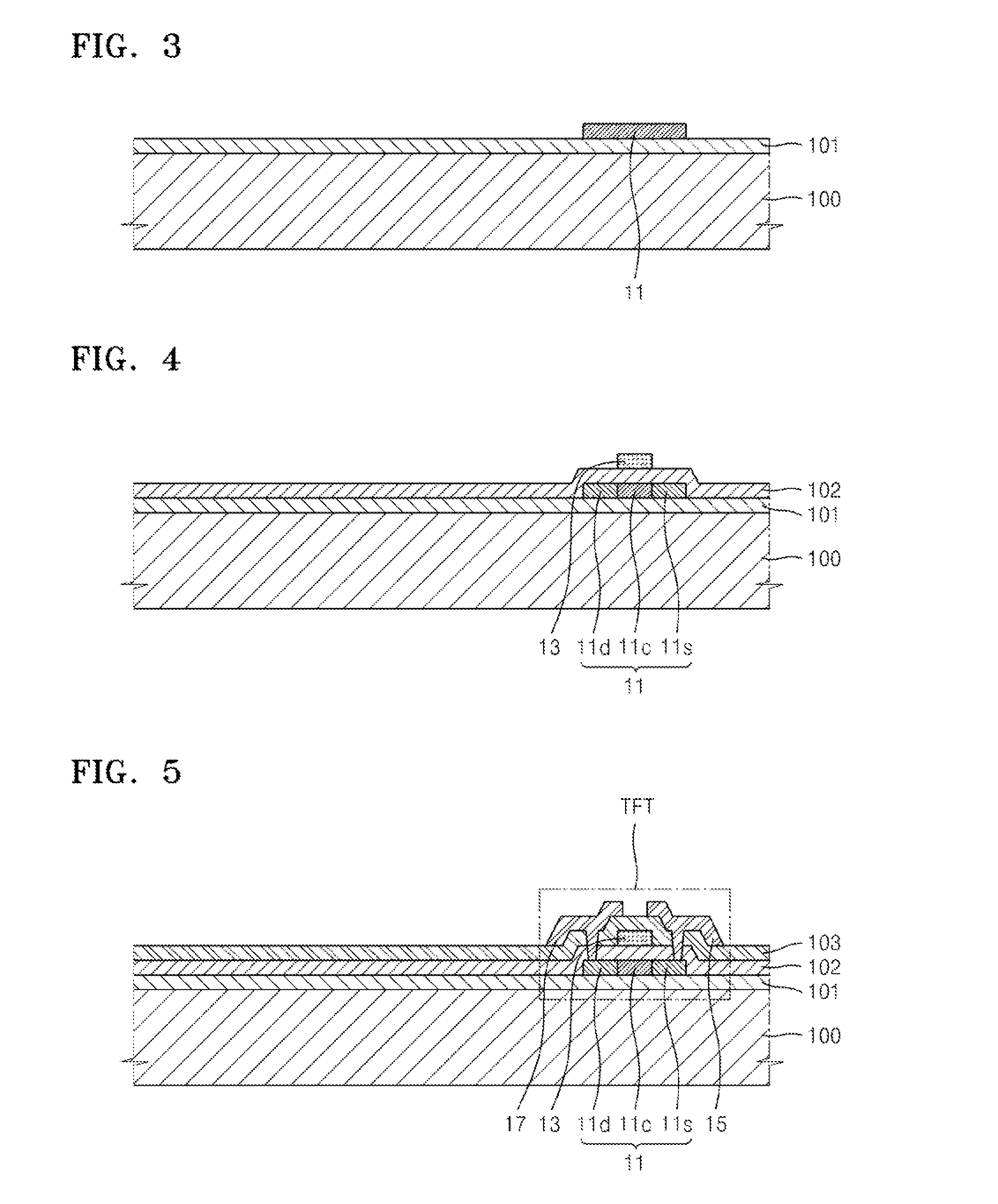
[0038]FIG. 1 is a schematic cross-sectional view illustrating an organic light emitting display apparatus 1 according to an embodiment of the present invention. Referring to FIG. 1, the organic light emitting display apparatus includes a thin film transistor TFT as a driving device, an organic light emitting device EL, and a contact area CNT. Although only one thin film transistor TFT is shown in FIG. 1, this is only for convenience of description, the present invention is not limit...


PUM


Abstract

An organic light emitting display apparatus includes pixel electrodes formed on a substrate for respective pixels. Auxiliary electrodes are formed on at least parts of the periphery of the pixel electrodes. A first organic function layer is formed on the substrate and covers the pixel electrodes and the auxiliary electrodes. An emissive layer is formed on the first organic function layer for the respective pixels. A second organic function layer is formed on the substrate and covers the emissive layer. A cathode electrode is formed on the entire substrate and faces the pixel electrodes and covers the second organic function layer. Secondary cathode electrodes are formed, on at least parts of the auxiliary electrodes, in contact with the cathode electrode through a contact hole.

Description

CROSS-REFERENCE TO RELATED PATENT APPLICATION[0001]This application claims the benefit of Korean Patent Application No. 10-2013-0057299, filed on May 21, 2013, in the Korean Intellectual Property Office, the disclosure of which is herein incorporated by reference in its entirety.TECHNICAL FIELD[0002]The present invention relates to a display, and more specifically, to an organic light emitting display apparatus and a method of manufacturing the same.DISCUSSION OF THE RELATED ART[0003]Organic light emitting display apparatuses have wide viewing angles and excellent contrasts. Additionally, these display apparatuses have fast response times.[0004]The organic light emitting display apparatuses include an organic layer, including a light emitting layer, between a pixel electrode and a cathode electrode which face each other. The cathode electrode is a common electrode and it applies the same voltage to all pixels. A voltage drop (IR drop) occurs within the cathode electrode due to a hig...

Claims


Application Information

Patent Timeline
IPC IPC(8): H01L51/52H01L51/56
CPCH01L51/56H01L51/5228H10K59/1315H10K71/60H10K50/824H05B33/10H10K71/00H10K50/805H10K59/131
Inventor SONG, JUNG-BAEJEONG, JIN-WOOK
Owner SAMSUNG DISPLAY CO LTD
Why Eureka
Try Eureka