Organic light emitting diode display and method of manufacturing the same

a light-emitting diode and display technology, applied in the field of flat-panel displays, can solve the problems of reducing the tensile stress and compressive stress, affecting the production efficiency of final products, and affecting the production efficiency of products, so as to reduce the interval, remove or reduce the abnormality of the picture, and selectively minimize the stress in the bent portion

Active Publication Date: 2014-11-27
SAMSUNG DISPLAY CO LTD
View PDF0 Cites 38 Cited by
  • Summary
  • Abstract
  • Description
  • Claims
  • Application Information

AI Technical Summary

Benefits of technology

[0028]According to the exemplary embodiments of the present invention, in an organic light emitting diode display, it is possible to selectively minimize stress in bent portions of an organic light emitting display panel by reducing an interval between stress adjustment patterns positioned corresponding to bent portions of the organic light emitting diode display panel. Therefore, asymmetry of strains of the bending portions of the organic light emitting diode display panel can be prevented to remove or reduce a picture abnormality.
[0029]Further, a stress adjustment layer is covered with a release film to flatten the lower passivation film before the stress adjustment layer of the lower passivation film is exposed. Thereby, it is possible to prevent a reduction in recognition ratio of an align mark due to optical scattering by the stress adjustment patterns of a lower passivation film during a manufacturing process.
[0030]Further, when a chip on film (COF

Problems solved by technology

When the flexible organic light emitting diode display is bent, stress occurs.
However, when the thickness of the organic light emitting diode display is increased by internal and external films such as a polarizing film and a passivation film attached to the organic light emitting diode display, the tensile stress and the compressive stress are increased and the neutral plane becomes displaced.
Accordingly, it is difficult to position the or

Method used


Image

  • Organic light emitting diode display and method of manufacturing the same
  • Organic light emitting diode display and method of manufacturing the same
  • Organic light emitting diode display and method of manufacturing the same

Examples


Embodiment Construction

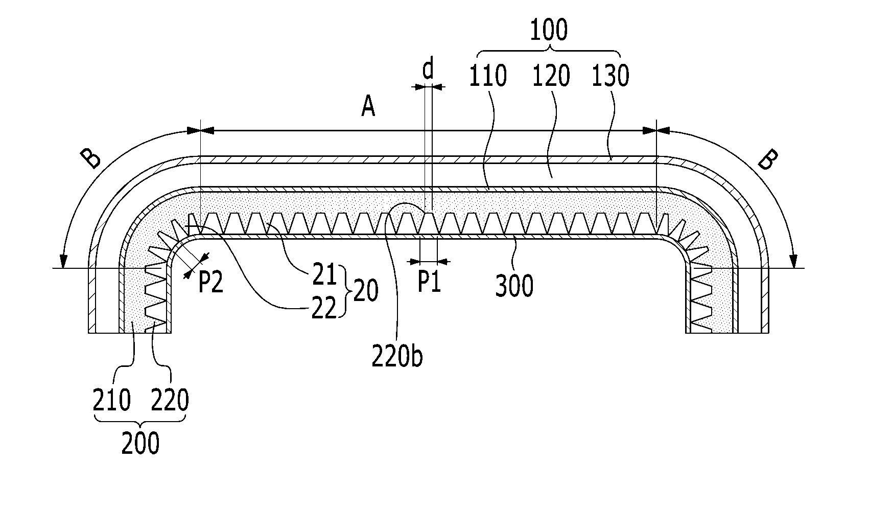
[0046]Hereinafter, exemplary embodiments of the present invention will be described in detail with reference to the accompanying drawings so that those skilled in the art may easily practice the present invention. As those skilled in the art would realize, the described embodiments may be modified in various different ways, all without departing from the spirit or scope of the present invention.

[0047]In describing the present invention, parts that are not related to the description will be omitted. Like reference numerals generally designate like elements throughout the specification.

[0048]In addition, the size and thickness of each element shown in the drawings are arbitrarily shown for understanding and ease of description, but the present invention is not limited thereto.

[0049]In the drawings, the thickness of layers, films, panels, regions, etc., are exaggerated for clarity. In the drawings, for understanding and ease of description, the thicknesses of some layers and areas are ...


PUM


Abstract

Disclosed is an organic light emitting diode display including an organic light emitting display panel configured to display an image, and a lower passivation film attached to a bottom of the organic light emitting diode display panel. The lower passivation film includes a support film that is in contact with the organic light emitting diode display panel, and a stress adjustment layer formed beneath the support film and configured to reduce a bending stress to be induced in the organic light emitting display panel when the organic light emitting display panel and the lower passivation film are bent.

Description

CROSS-REFERENCE TO RELATED APPLICATION[0001]This application claims priority to, and the benefit of, Korean Patent Application Nos. 10-2013-0106747 and 10-2013-0057249 filed in the Korean Intellectual Property Office on Sep. 5, 2013 and May 21, 2013 respectively, the entire contents of each of which are incorporated herein by reference.BACKGROUND OF THE INVENTION[0002](a) Field of the Invention[0003]Embodiments of the present invention relate generally to flat panel displays. More specifically, embodiments of the present invention relate to an organic light emitting diode display and a method of manufacturing the same.[0004](b) Description of the Related Art[0005]An organic light emitting diode display includes organic light emitting elements that each have a hole injection electrode, an organic light emitting layer, and an electron injection electrode. Each organic light emitting element emits light due to energy generated when an exciton generated by combining electrons and holes ...

Claims


Application Information

Patent Timeline
IPC IPC(8): H01L51/52H01L27/32H01L51/56
CPCH01L51/5253H01L27/32H01L51/56Y02E10/549Y02P70/50H10K59/00H10K50/841H10K50/844H10K71/00H10K2102/311H10K50/84H10K59/12H10K77/10
Inventor JEONG, CHUL WOOPARK, SOON RYONGSO, JUNG HOBAEK, SEOK GIKIM, KWANG HYEOKEOM, JEONG YONG
Owner SAMSUNG DISPLAY CO LTD
Why Eureka
Try Eureka