Semiconductor device and method for manufacturing semiconductor device

Active Publication Date: 2014-11-27
FUJI ELECTRIC CO LTD
View PDF6 Cites 47 Cited by
  • Summary
  • Abstract
  • Description
  • Claims
  • Application Information

AI Technical Summary

Benefits of technology

[0015]Embodiments of the invention provide a semiconductor device and a semiconductor device manufacturing method which can ensur

Problems solved by technology

However, in this case, the electrical connection between the two mold cases is not considered at all and there is an unsolved problem that the device cannot be applied as a power conversion semiconductor device.
Therefore, when the inverter device is formed, two screwing processes, that is, a process of screwing the main elements to the radiation fin and a process of screwing the main circuit boards to the upper surfaces of each main element for an upper arm and each main element for a lower arm are required and there is an unsolved problem that it takes a lot of time for the attachment operation.
Therefore, the leaf spring for pressure and the reinforcing beam are required to bring a plurality of semiconductor modules into close contact with the heat sink and it is difficult to

Method used


Image

  • Semiconductor device and method for manufacturing semiconductor device
  • Semiconductor device and method for manufacturing semiconductor device
  • Semiconductor device and method for manufacturing semiconductor device

Examples


Example

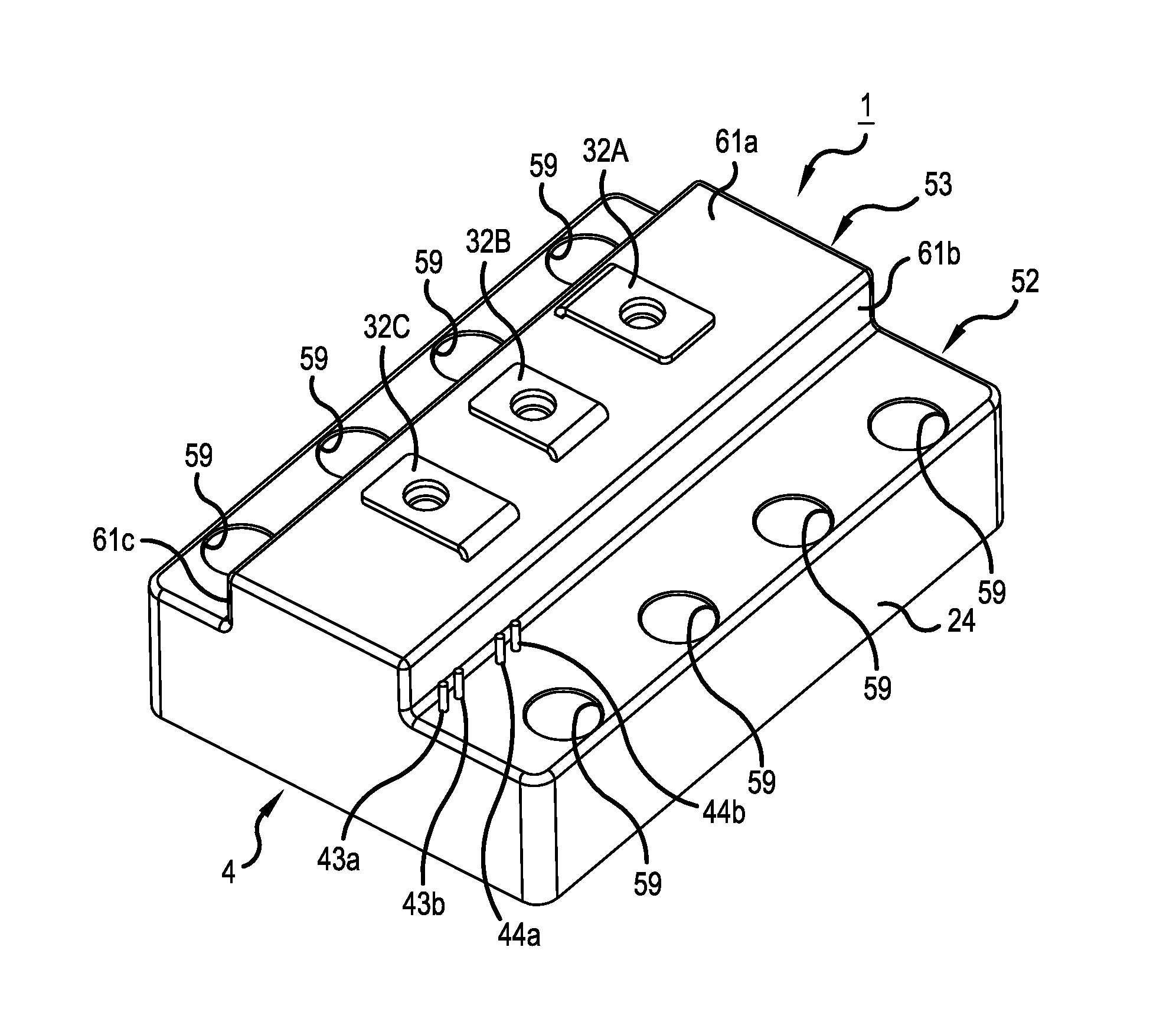
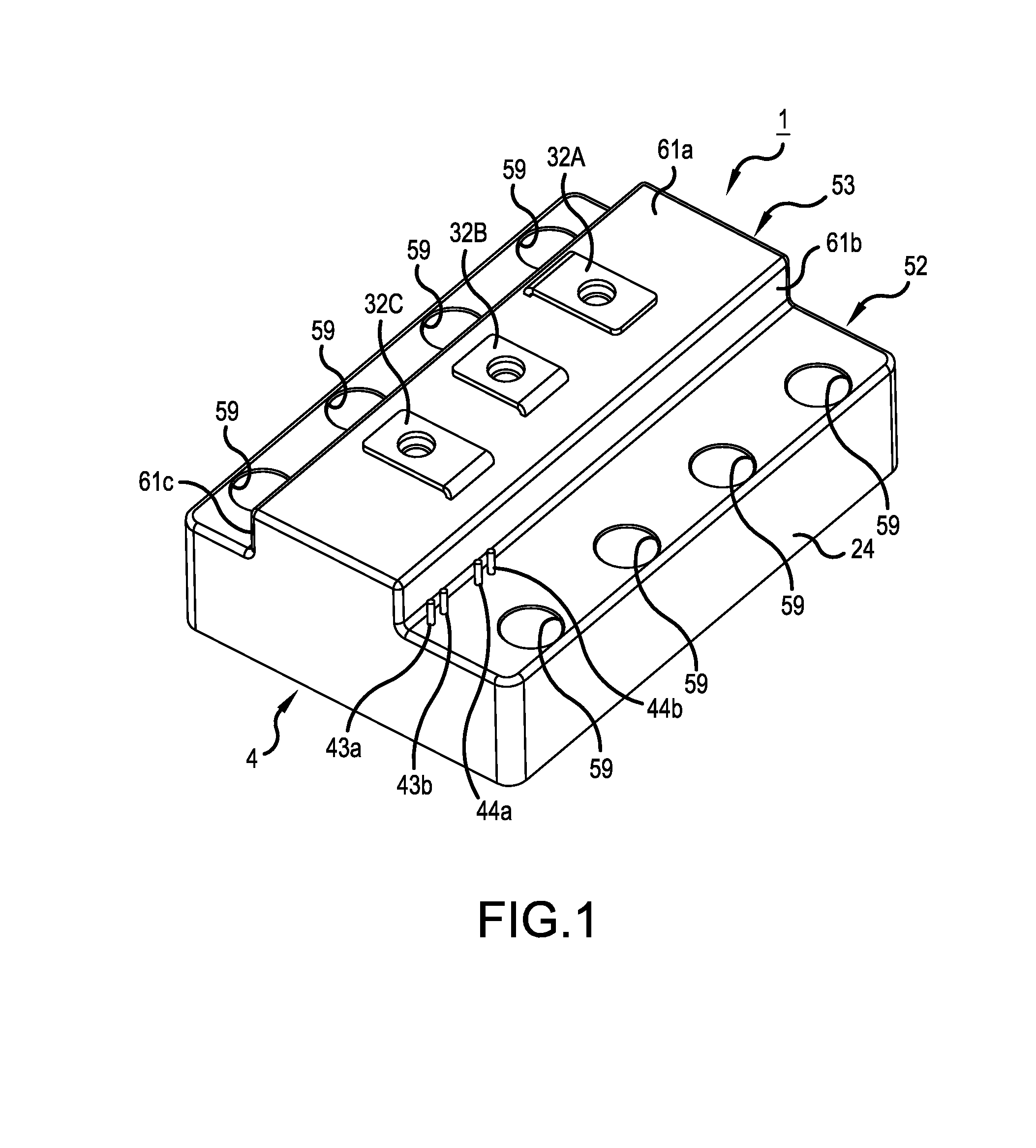
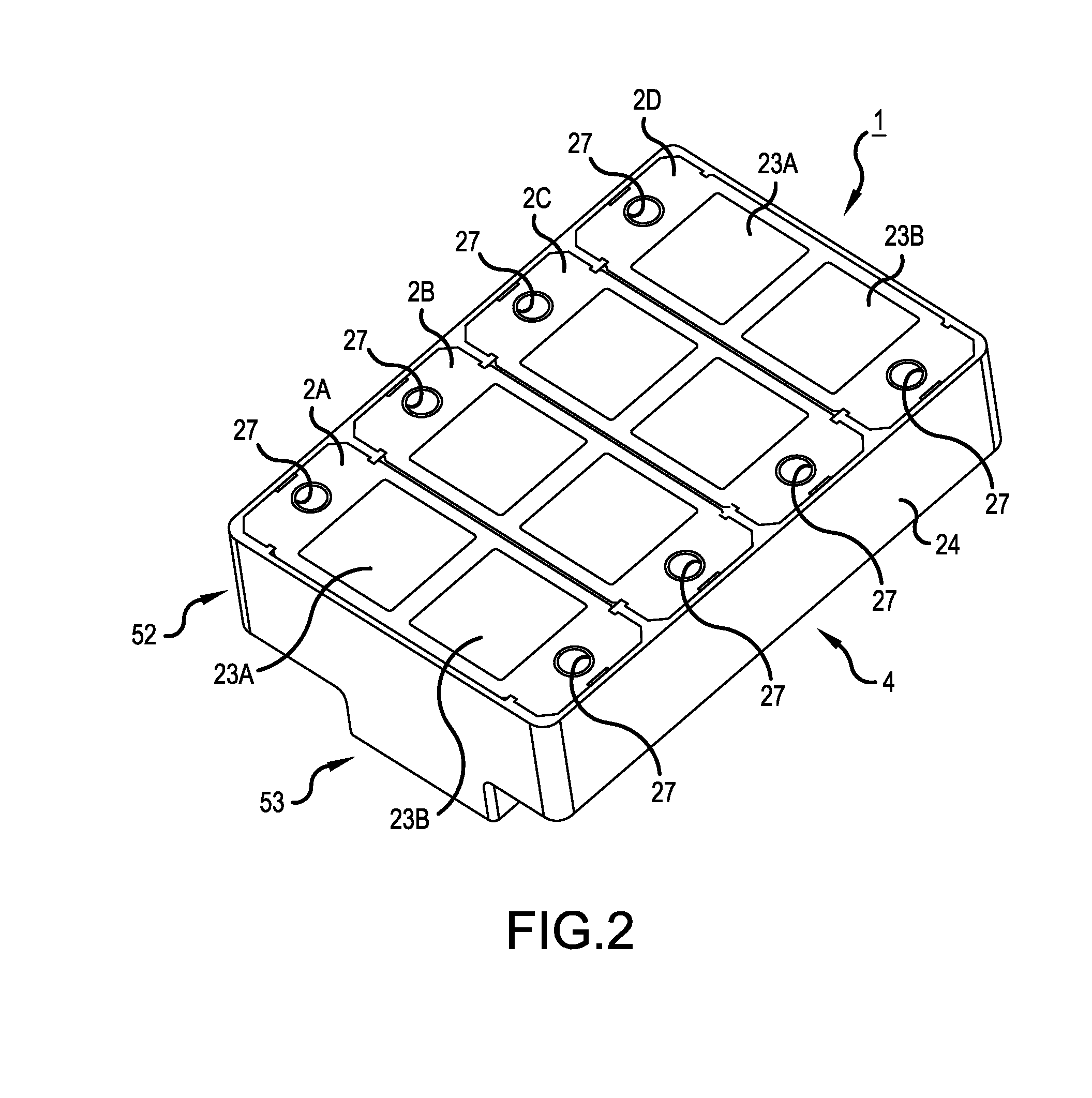
[0049]Hereinafter, embodiments of the invention will be described with reference to the drawings. FIG. 1 is a perspective view illustrating the top side of a semiconductor device according to an embodiment of the invention and FIG. 2 is a perspective view illustrating the bottom side of the semiconductor device. FIG. 3 is an exploded perspective view illustrating the semiconductor device. FIG. 4 is a plan view illustrating the semiconductor device. FIG. 5 is a cross-sectional view taken along the line A-A of FIG. 3 and FIG. 6 is a cross-sectional view taken along the line B-B of FIG. 3. As illustrated in FIG. 3, a semiconductor device 1 includes a plurality of power semiconductor modules, for example, four power semiconductor modules 2A to 2D, three main terminal plates 3A to 3C that individually connect connection terminals of the power semiconductor modules 2A to 2D, and a module storage case 4 that accommodates the power semiconductor modules 2A to 2D and the main terminal plate ...


PUM


Abstract

A semiconductor device includes: semiconductor modules in which a circuit board having at least one or more semiconductor chips mounted thereon is sealed with a mold resin material and an attachment hole is formed; main terminal plates that individually connect individual connection terminals of the plurality of semiconductor modules which are arranged in parallel; and a module storage case into which the plurality of the semiconductor modules connected by the main terminal plates are inserted integrally with the main terminal plates from an opening portion and which holds the plurality of semiconductor modules such that the position of the semiconductor modules can be adjusted during attachment and includes attachment insertion holes facing the attachment holes of the semiconductor modules.

Description

CROSS REFERENCE TO RELATED APPLICATIONS[0001]This application is a continuation of International Application No. PCT / JP2013 / 001804, filed on Mar. 15, 2013, which is based on and claims priority to Japanese Patent Application No. JP 2012-072673, filed on Mar. 28, 2012 and Japanese Patent Application No. JP 2012-182614, filed on Aug. 21, 2012. The disclosure of the Japanese priority applications and the PCT application in their entirety, including the drawings, claims, and the specification thereof, are incorporated herein by reference.BACKGROUND[0002]1. Field of the Invention[0003]Embodiments of the present invention relate to a semiconductor device that includes a plurality of semiconductor modules including, for example, a power device and a method for manufacturing a semiconductor device.[0004]2. Discussion of the Background[0005]A power conversion inverter device has been widely used as one of power conversion devices. For example, an electric motor is generally used as a driving...

Claims


Application Information

Patent Timeline
IPC IPC(8): H01L23/36H01L25/065H01L23/08
CPCH01L23/36H01L25/0655H01L23/08H01L25/18H02M7/003H01L25/072H05K7/209H01L23/043H01L23/5385H01L23/3735H01L23/4334H01L23/4006H01L25/115H01L2224/16225H01L2924/10253H01L2924/10272H01L2924/13055H01L2924/1421H01L2924/13091H05K7/14329H01L2924/00H05K7/1432
Inventor NAKAMURA, HIDEYOHORIO, MASAFUMI
Owner FUJI ELECTRIC CO LTD
Why Eureka
Try Eureka