

Semiconductor integrated circuit device and high-frequency power amplifier module
a technology of integrated circuit device and high-frequency power amplifier, which is applied in the direction of amplifier with semiconductor device/discharge tube, amplification control details, gated amplifier, etc., can solve the problems of complex combination management, risk of transmission power characteristics variation, and certain level of error between high-frequency power amplifier devices
- Summary
- Abstract
- Description
- Claims
- Application Information
AI Technical Summary
Benefits of technology
Problems solved by technology
Method used
Image

Examples
embodiment 1
Total Configuration of Mobile Phone System (Wireless Communication Systems)
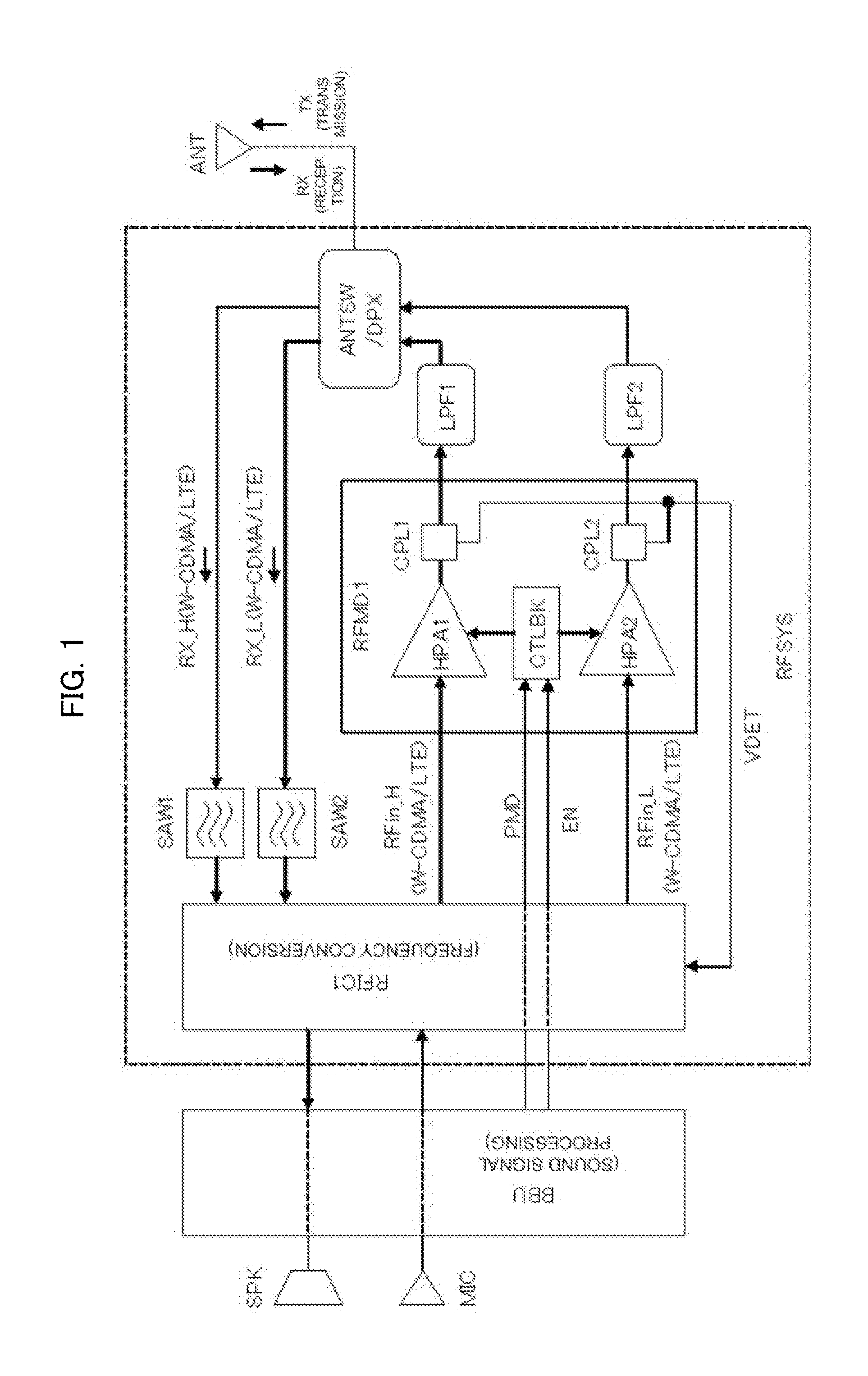
[0038]FIG. 1 is a block diagram illustrating a configuration example of a mobile phone system to which reduction of variations in the transmission characteristics is applied in a wireless communication system according to Embodiment 1 of the present invention. A mobile phone system in FIG. 1 includes a baseband unit BBU, a high-frequency system unit RFSYS, an antenna ANT, a speaker SPK, a microphone MIC, and the like. The BBU converts an analog signal into a digital signal to be used in the SPK and the MIC, performs various digital signal processes (modulation, demodulation, digital filtering, etc.) associated with communications, and outputs various control signals associated with the communications. Among the various control signals, there are included a power mode selection signal PMD for switching a transmission power mode, and a band selection signal EN for selecting a frequency band (band).
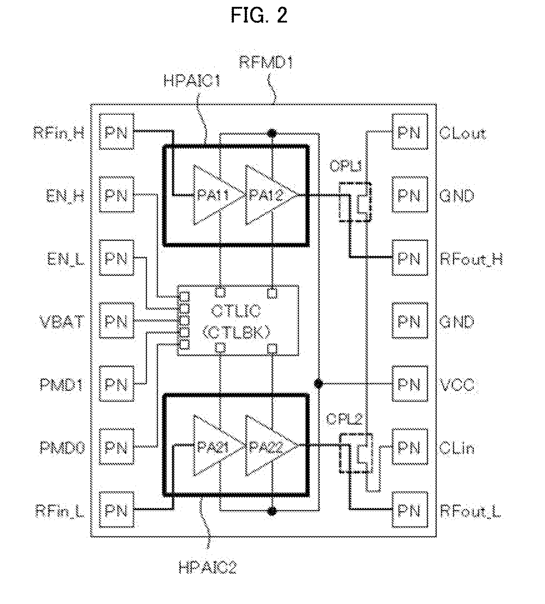
[0039]The hig...
embodiment 2
Detailed Configuration of the Reference-Voltage Correction Circuit (Modification [1])
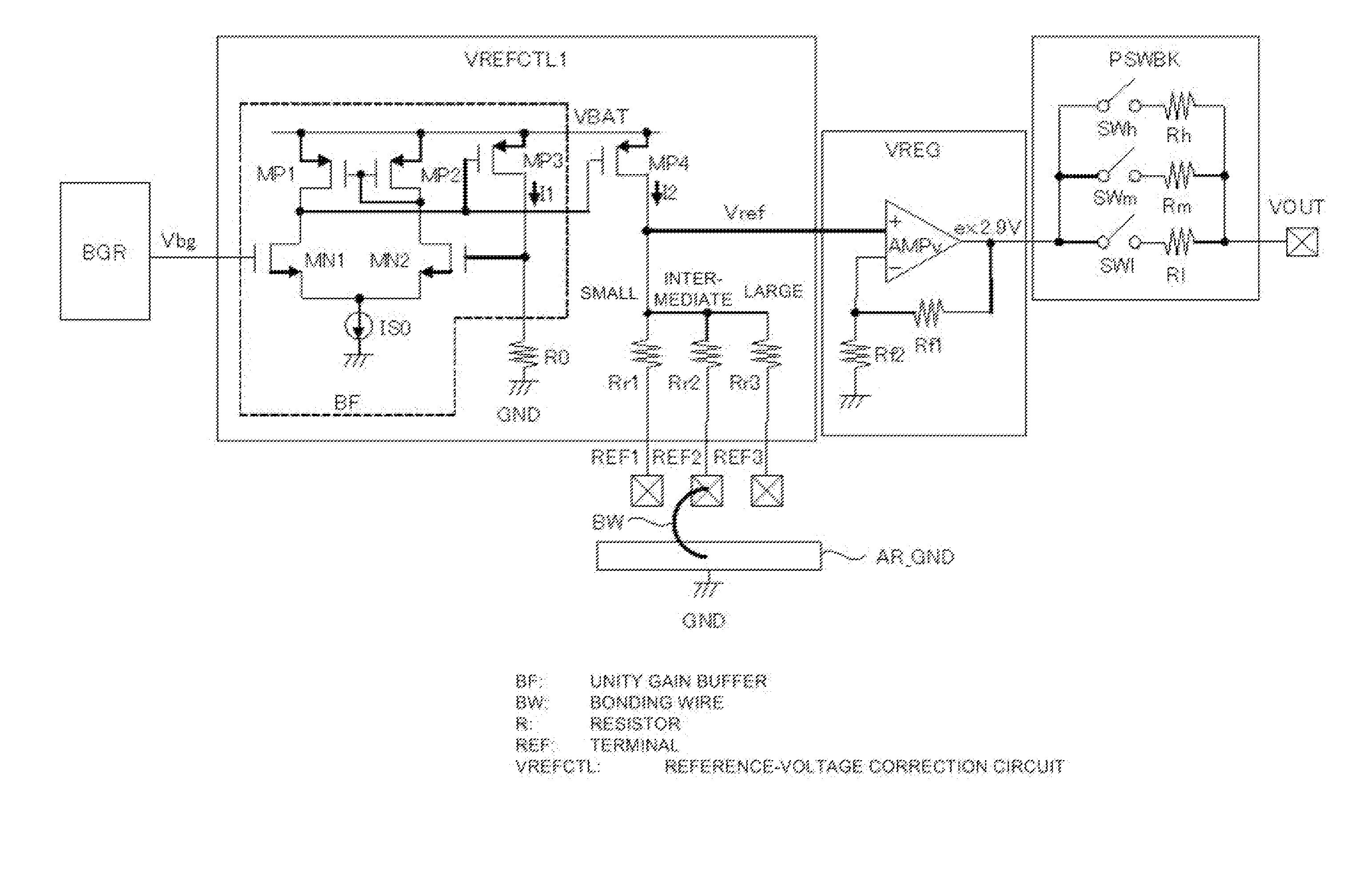
[0087]FIG. 11 is a circuit diagram illustrating a detailed configuration example of a reference-voltage correction circuit in a control chip included in a high-frequency power amplifier module according to Embodiment 2 of the present invention. A reference-voltage correction circuit VREFCTL2 illustrated in FIG. 11 Is a modification of the VREFCTL1 in FIG. 4, and includes a comparator circuit block CMPBK1 and the switch block SWBK1, in addition to the unity gain buffer BF, the PMOS transistor MP4, the resistors R0, and Rr1 to Rr3 that are similar to those in FIG. 4.
[0088]The switch block SWBK1 includes switches SWr1 to SWr3. The SWr1 is connected between the drain of the PMOS transistor MP4 and one end of the resistor Rr1, the SWr2 is connected between the drain of the MP4 and one end of the resistor Rr2, and the SWr3 is connected between the drain of the MP4 and one end of the resistor Rr3. The othe...
embodiment 3
Detailed Configuration of the Reference-Voltage Correction Circuit (Modification [2])
[0092]FIG. 14 is a circuit diagram illustrating a detailed configuration example of a reference-voltage correction circuit in a control chip included in a high-frequency power amplifier module according to Embodiment 3 of the present invention. A reference-voltage correction circuit VREFCTL3 illustrated in FIG. 14 is a modification of the VREFCTL1 in FIG. 4, and includes a comparator circuit block CMPBK2, a switch block SWBK2, a resistor Rr3′, and a fuse FS, in addition to the unity gain buffer BF, the PMOS transistor MP4, the resistors R0, and Rr1, and Rr2 that are similar to those in FIG. 4.
[0093]The switch block SWBK2 includes switches SWr1 and SWr23. The SWr1 is connected between the drain of the PMOS transistor MP4 and one end of the resistor Rr1, and the SWr23 is connected between the drain of the MP4 and one end of the resistor Rr2. The other end of the Rr1 is connected to the ground power su...
PUM
 Abstract
Description
Claims
Application Information