Optical Circuit Board

a technology of optical circuit boards and printed circuit boards, applied in the direction of optical waveguide light guides, instruments, optical elements, etc., can solve the problems of difficult to guarantee good signal integrity, the limit of electrical communication between printed circuit boards (pcbs) is reached

Inactive Publication Date: 2014-11-27
YABRE GNITABOURE
View PDF14 Cites 14 Cited by
  • Summary
  • Abstract
  • Description
  • Claims
  • Application Information

AI Technical Summary

Benefits of technology

[0013]With these features, efficient thermal management of the opto-electronic component is provided at the board, using the heat dissipative element, which enables new gains in terms of data rates.

Problems solved by technology

Because of the ever increasing requirements in data rates in communication systems, due for example to the Internet, the limits of using electrical communications between printed circuit boards (PCB) are being reached.
It has become difficult to guarantee good signal integrity when transferring information at high frequencies (e.g. 25 Gb / s or higher) through electrical lines between two electrical components such as a printed circuit board.

Method used


Image

  • Optical Circuit Board
  • Optical Circuit Board
  • Optical Circuit Board

Examples


second embodiment

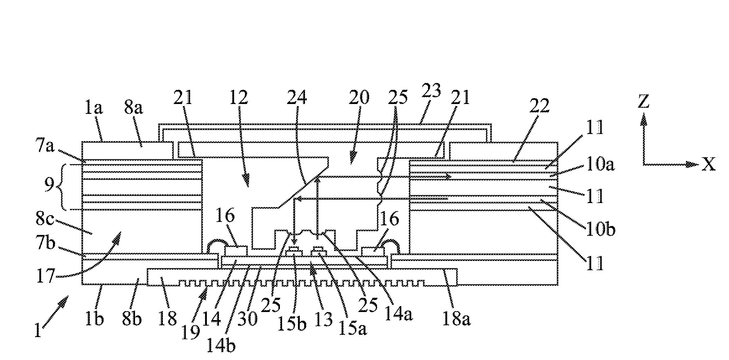
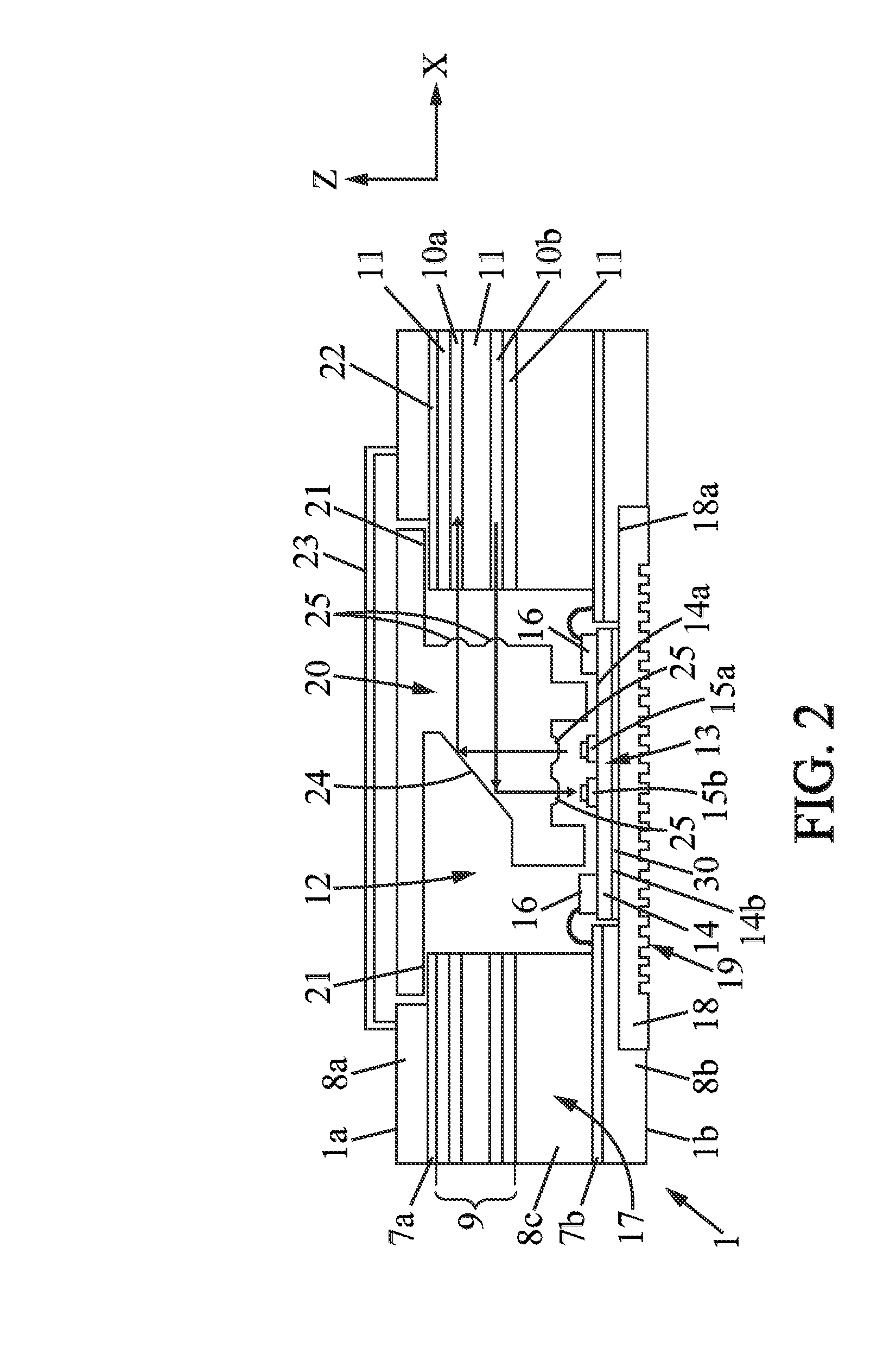
[0040]FIG. 3 now shows the invention. Compared to the embodiment of FIG. 2, the embodiment of FIG. 3 differs in that one does not use a heat-dissipating printed circuit board 14. It does not either use a heat spreader. In the following embodiments, as well as in the above embodiment, the heat spreader may be optional. Thus, the opto-electrical components 15a, 15b are directly fixed to the heat sink 18. The opto-electrical components 15a, 15b are connected electrically to an electrical track of the system card 1, such as the bottom card 7b, by wire bonding. The electronic control components 16 are therefore provided directly on the body of the system card and electrically connected to the electrical layer 7b by any suitable way.

third embodiment

[0041]FIG. 4 now shows a Compared to the embodiment of FIG. 3, the main difference lies in the geometry of the optical coupling device 20. There will be a longer optical path inside the optical coupling device, for example by providing a plurality of mirrors 24, 24b, 24c between the interfaces of the optical coupling device. The optical coupling device 20 may even project from the top face 1a of the board 1, and light may even propagate inside the optical coupling device in a plane higher along direction Z, than the top face 1a of the card 1.

fourth embodiment

[0042]FIG. 5 now shows a Compared to the embodiment of FIG. 3, it differs in that the opto-electrical components 15a, 15b are electrically connected to the top electrical layer 7a of the board 1. Two cavities 12a, 12b are provided in the body 17 of the card 1. The cavity 12a receives the heat sink 18 which extends also at the level of the optical layer 9, up to the top electrical layer 7a. The second cavity 12b receives a portion of the optical coupling device 20. Light emitted from a laser 15a along direction Z upward is reflected by a first mirror 24a to propagate inside the coupling device 20 along direction X toward the left until it reaches a second mirror 24b where it is reflected along direction Z downwards, until a third mirror 24c, which extends in the second cavity 12b, directs light leftward again, along direction X, to the suitable optical waveguide 10b. In the present embodiment, light will propagate on the left hand side part of the optical layer 9. Light directed fro...


PUM


Abstract

An optical circuit board including a top face, a bottom face, an optical layer buried between bottom and top faces, the optical layer being adapted to transmit optical signals, an opto-electronic component adapted to emit or receive light transmitted through the optical layer, a solid heat dissipative element adapted to dissipate heat generated at the opto-electronic component.

Description

FIELD OF THE INVENTION[0001]The instant invention relates to optical circuit boards.BACKGROUND OF THE INVENTION[0002]Today, most communication systems involve a number of system-cards. Such cards are usually manufactured as so-called printed circuit boards (PCBs). Usually, some of the system-cards, which are called daughter boards, are assembled together on a rigid system-card called the backplane, or mother board.[0003]The daughter boards usually extend parallel with each other and are interconnected together via the backplane, which extends perpendicular to them. There are several practical advantages to such a configuration: Easy insertion, removal, and replacement of the daughter-boards.[0004]Because of the ever increasing requirements in data rates in communication systems, due for example to the Internet, the limits of using electrical communications between printed circuit boards (PCB) are being reached. It has become difficult to guarantee good signal integrity when transfer...

Claims


Application Information

Patent Timeline
Patent Type & Authority Applications(United States)
IPC IPC(8): G02B6/42
CPCG02B6/4272G02B6/4212G02B6/4214G02B6/4269G02B6/42G02B6/423G02B6/4234G02B6/4246H01L2224/48091H01L2924/00014
Inventor YABRE, GNITABOURE
Owner YABRE GNITABOURE
Why Eureka
Try Eureka