Transmission electron microscope sample fabrication

a technology of transmission electron microscope and sample, applied in the direction of material analysis using wave/particle radiation, instruments, nuclear engineering, etc., can solve the problems of obfuscating features, tem sample preparation challenges may become more prevalent, and conventional transmission electron microscopy (tem) techniques may not be able to generate the thin sample thickness required for clearly imaging such structures, etc., to achieve the effect of improving the tem sample preparation process

Inactive Publication Date: 2014-12-04
GLOBALFOUNDRIES INC
View PDF8 Cites 11 Cited by
  • Summary
  • Abstract
  • Description
  • Claims
  • Application Information

AI Technical Summary

Benefits of technology

[0006]It may, therefore, be desirable, among other things, to provide enhanced TEM sample preparation processes.

Problems solved by technology

Based on Moore's Law's the shrinking dimensions of, for example, semiconductor device structures (e.g., Field Effect Transistors), conventional transmission electron microscopy (TEM) techniques may be incapable of generating the thin sample thicknesses required for clearly imaging such structures.
Accordingly, TEM sample preparation challenges may become more prevalent.
This in turn may lead to projection effects which can obfuscate the features of interest and, thus, mask critical information associated with the fabricated sample.

Method used


Image

  • Transmission electron microscope sample fabrication
  • Transmission electron microscope sample fabrication
  • Transmission electron microscope sample fabrication

Examples


Embodiment Construction

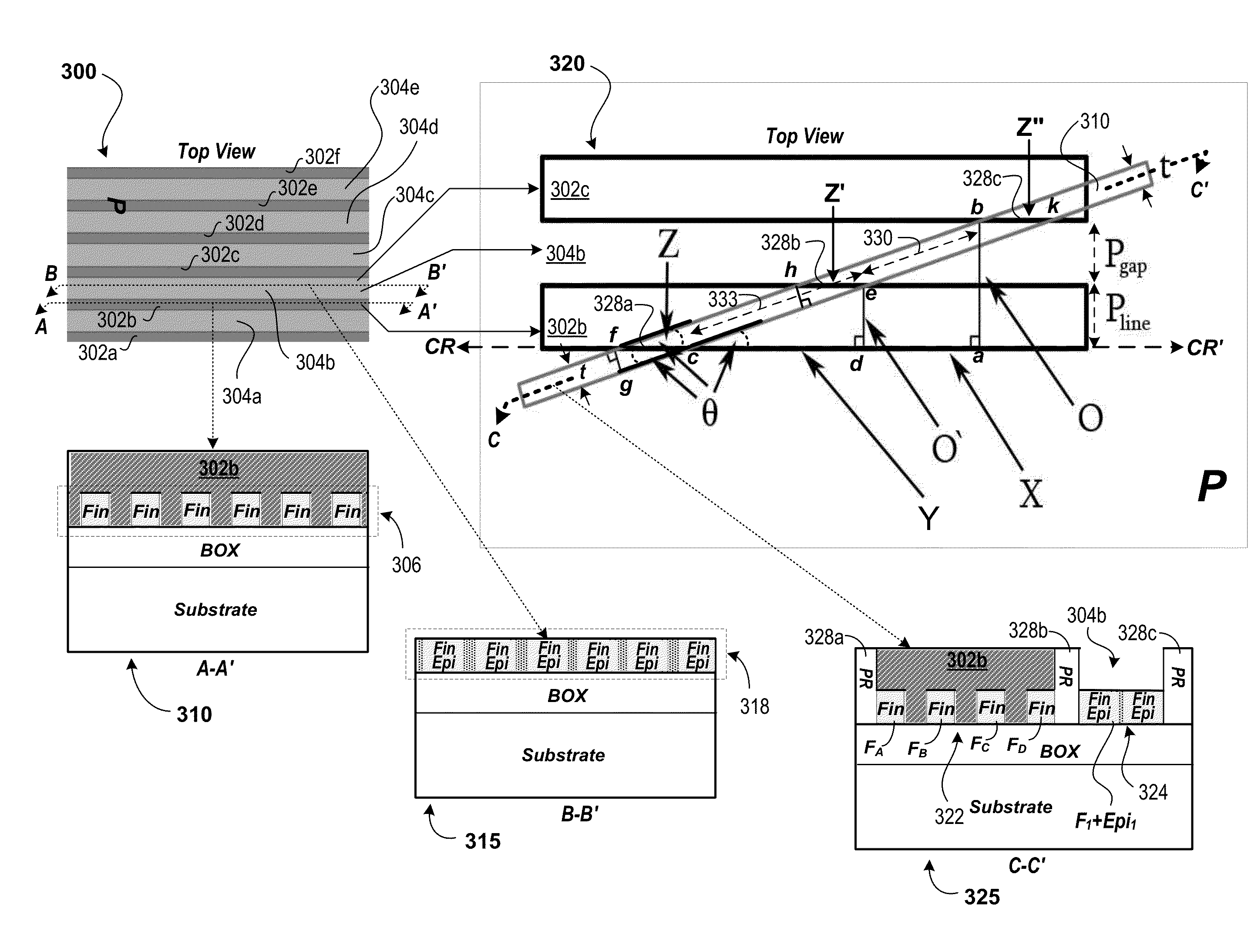
[0017]The following one or more exemplary embodiments describe a method of preparing a transmission electron microscopy (TEM) sample corresponding to a semiconductor device in a manner that enables a TEM image of the sample to include image projection-free regions. In particular, the one or more exemplary embodiments described below may be directed to mitigating or removing image projection effect while imaging, for example, device structural dimensions or 50 nm or less. Example device structures may include 3-dimensional semiconductor device structures such as FinFET devices.

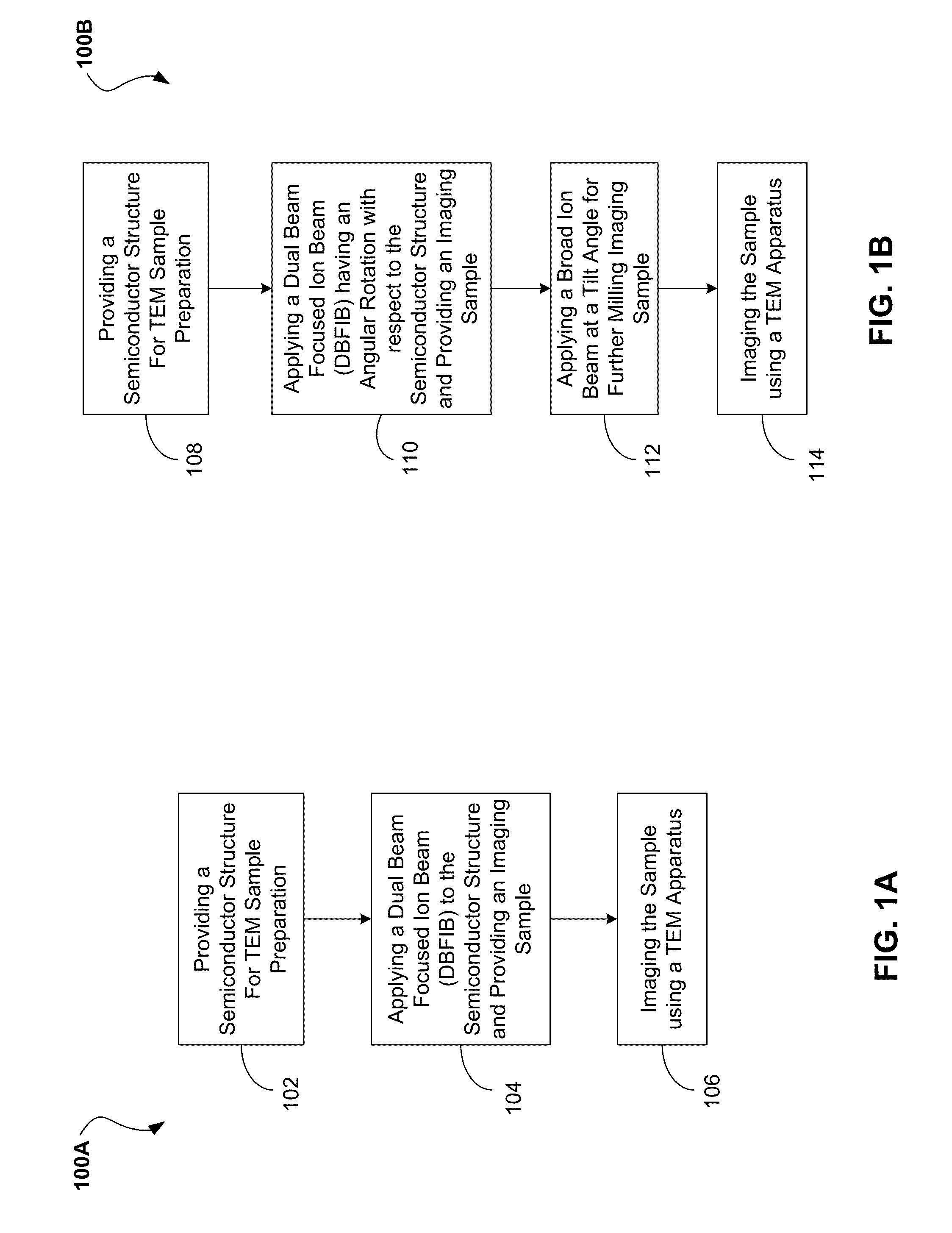
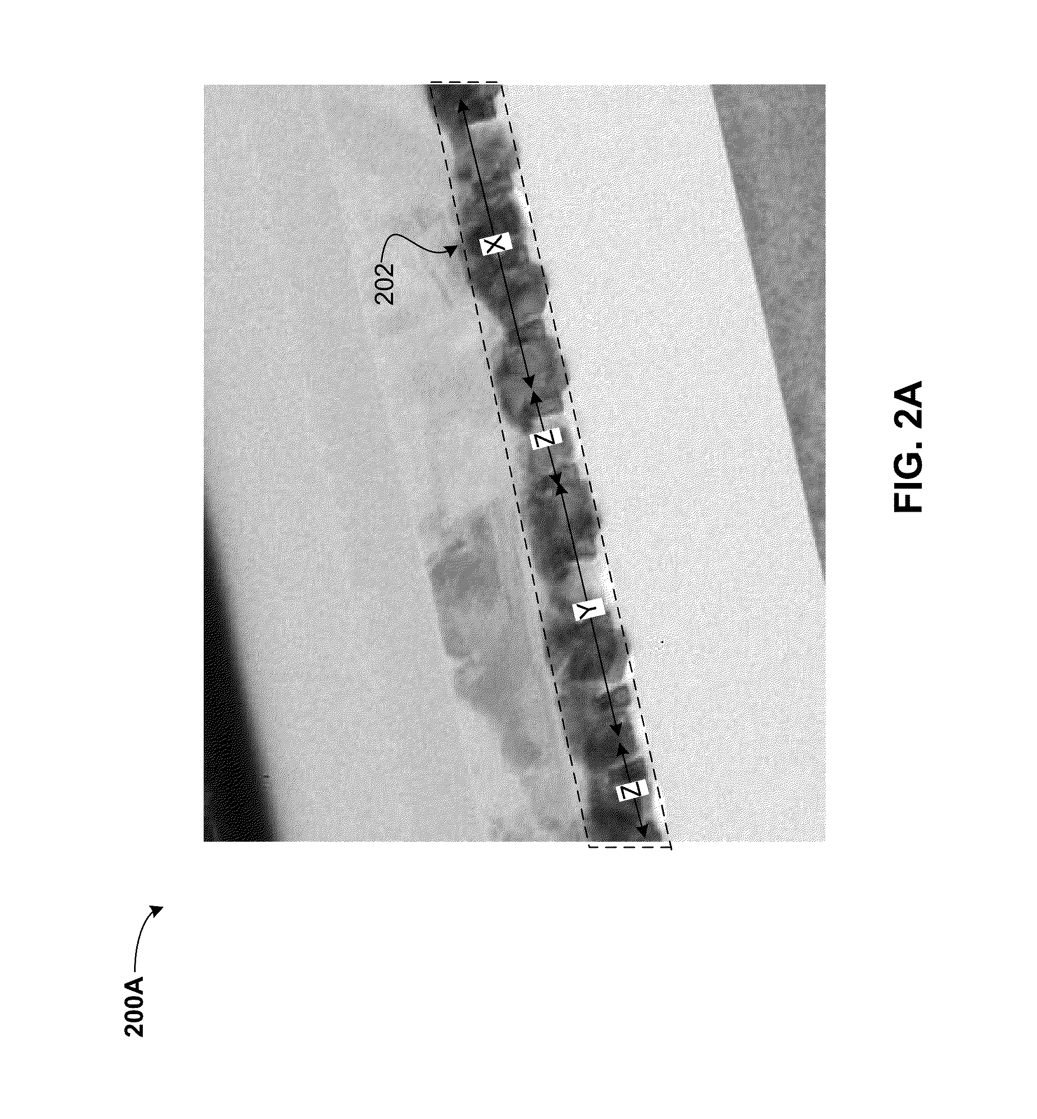
[0018]FIG. 1A depicts an operational flow diagram 100A for preparing a TEM sample according to conventional methods. FIG. 1A will be described with aid of FIG. 2A and FIG. 3. At 102, a semiconductor structure such as semiconductor structure 300 (FIG. 3) is provided for preparing a TEM sample within a region of interest. For example, the region of interest may include a plurality of fin structures associated wit...


PUM

PropertyMeasurementUnit
rotationaaaaaaaaaa
spot sizeaaaaaaaaaa
lengthaaaaaaaaaa

Abstract

A method of preparing a transmission electron microscopy (TEM) sample from a semiconductor structure may include milling a region of the semiconductor structure with a focused ion beam and generating the transmission electron microscopy (TEM) sample. The focused ion beam providing the milling may include a rotation angle relative to the crystallographic axis of the semiconductor structure. A transmission electron microscopy image of a cross-sectional plane of the generated transmission electron microscopy (TEM) sample may be generated using a transmission electron microscope, whereby the transmission electron microscopy image of the cross-sectional plane includes an image projection-free region based on the rotation angle.

Description

BACKGROUND[0001]a. Field of the Invention[0002]The present invention generally relates to semiconductor device imaging, and more particularly, to the preparation of semiconductor devices for such device imaging processes.[0003]b. Background of Invention[0004]Based on Moore's Law's the shrinking dimensions of, for example, semiconductor device structures (e.g., Field Effect Transistors), conventional transmission electron microscopy (TEM) techniques may be incapable of generating the thin sample thicknesses required for clearly imaging such structures. Accordingly, TEM sample preparation challenges may become more prevalent.[0005]Automated TEM sample fabrication with instruments such as single and dual beam focused ion beams may include lamella thicknesses in the region of 100 nm. However, device and test structure dimensions may now contain multiple features within a 100 nm slice. This in turn may lead to projection effects which can obfuscate the features of interest and, thus, mas...

Claims


Application Information

Patent Timeline
Patent Type & Authority Applications(United States)
IPC IPC(8): G01N1/28
CPCG01N1/28G01N1/32H01J2237/31745H01J2237/31749H01J2237/20214H01J2237/20207H01J37/31H01J37/26
Inventor DEMAREST, JAMES J.LI, JUNTAO
Owner GLOBALFOUNDRIES INC
Why Eureka
Try Eureka