

Semiconductor device, method of manufacturing semiconductor device, solid-state imaging unit, and electronic apparatus
- Summary
- Abstract
- Description
- Claims
- Application Information
AI Technical Summary
Benefits of technology
Problems solved by technology
Method used
Image

Examples
application example 2 (
8. Application Example 2 (An example of an electronic apparatus (a camera))
embodiment
1. Embodiment
[Configuration]
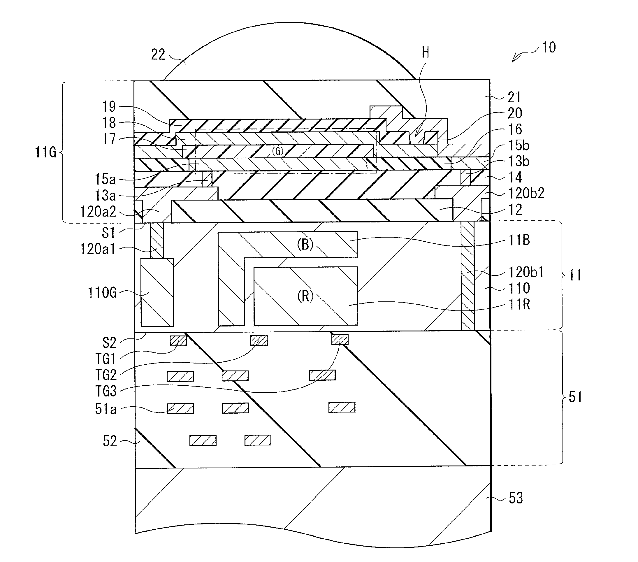
[0062]FIG. 1 illustrates a cross-sectional configuration of a semiconductor device (a photoelectric conversion device 10) of an embodiment of the present disclosure. The photoelectric conversion device 10 may configure, for example, one pixel in a solid-state imaging unit (which will be described later) such as a CCD image sensor and a CMOS image sensor.
[0063]In the photoelectric conversion device 10, pixel transistors (including transfer transistors Tr1 to Tr3 which will be described later) are formed and a multi-layered wiring layer (a multi-layered wiring layer 51) is provided on a front face (a surface S2 on an opposite side from a light receiving surface) side of a semiconductor substrate 11.
[0064]This photoelectric conversion device 10 has a structure in which an organic photoelectric conversion section and an inorganic photoelectric conversion section are laminated in a vertical direction. The organic photoelectric conversion section and the inorga...
modification 1
[0135]FIG. 25 to FIG. 29 illustrate a method of manufacturing a photoelectric conversion device (a method of processing the upper electrode 18) according to Modification 1 in order of steps. In the processing method in the present modification, the protective film 19 formed on the upper electrode 18 is patterned, and then, this patterned protective film 18 is used as a mask to etch the upper electrode 18. It is to be noted that the method of forming the semiconductor substrate 11 and the unillustrated wiring layer 51 and support substrate 53 is similar to that in the above-described embodiment.
[0136]Specifically, first, as in the above-described embodiment, as shown in FIG. 25, the upper electrode 18 is formed so as to cover the organic photoelectric conversion layer 17. At this time, the upper electrode 18 is formed to cover the top face and the side faces of the organic photoelectric conversion layer 17 as described above.
[0137]Subsequently, as shown in FIG. 26, a protective film ...
PUM
 Abstract
Description
Claims
Application Information