

Metal gate transistor and method for forming the same
- Summary
- Abstract
- Description
- Claims
- Application Information
AI Technical Summary
Benefits of technology
Problems solved by technology
Method used
Image

Examples
Embodiment Construction
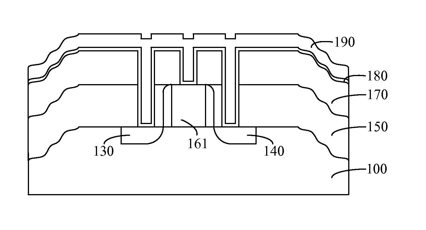
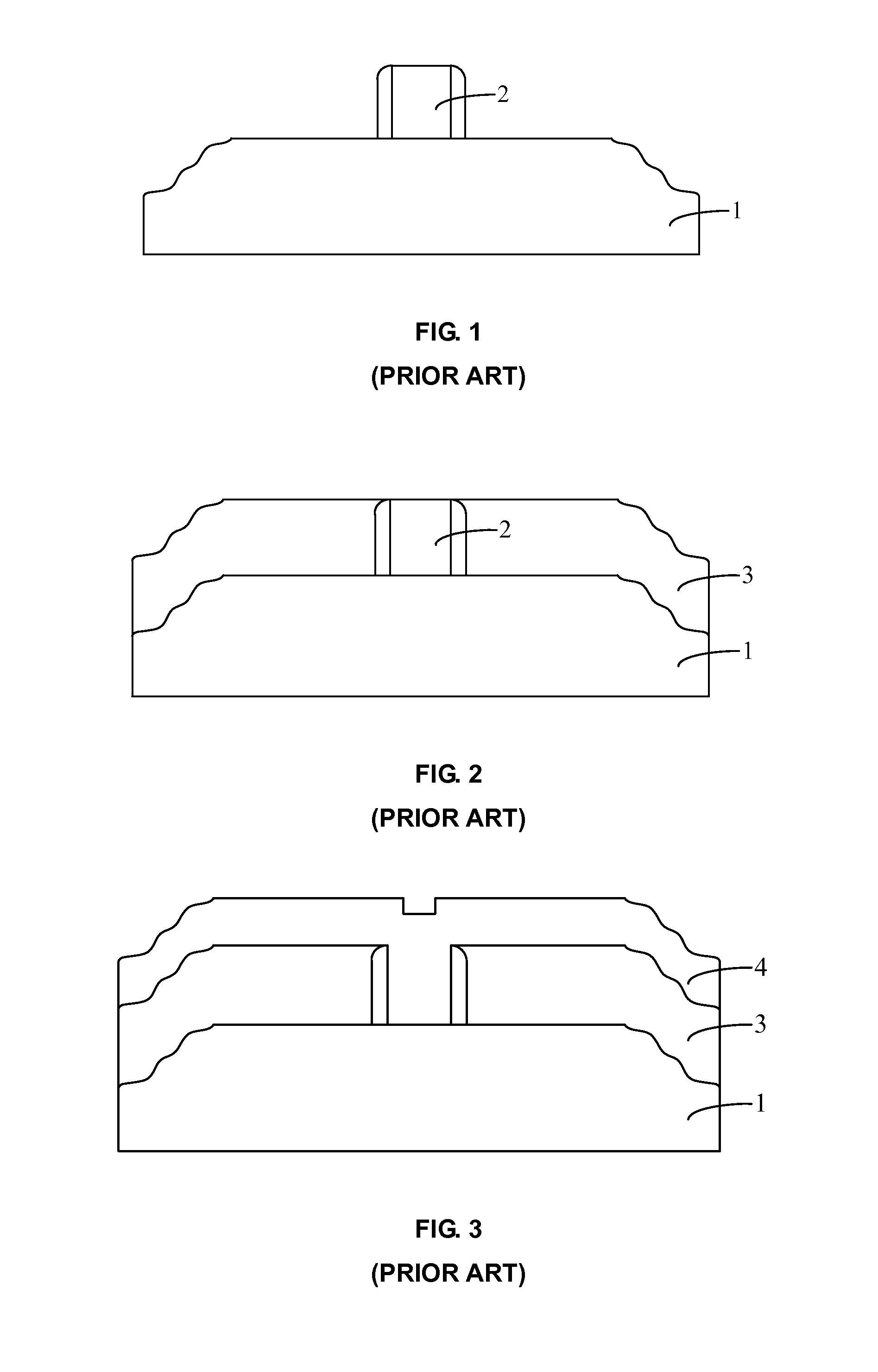
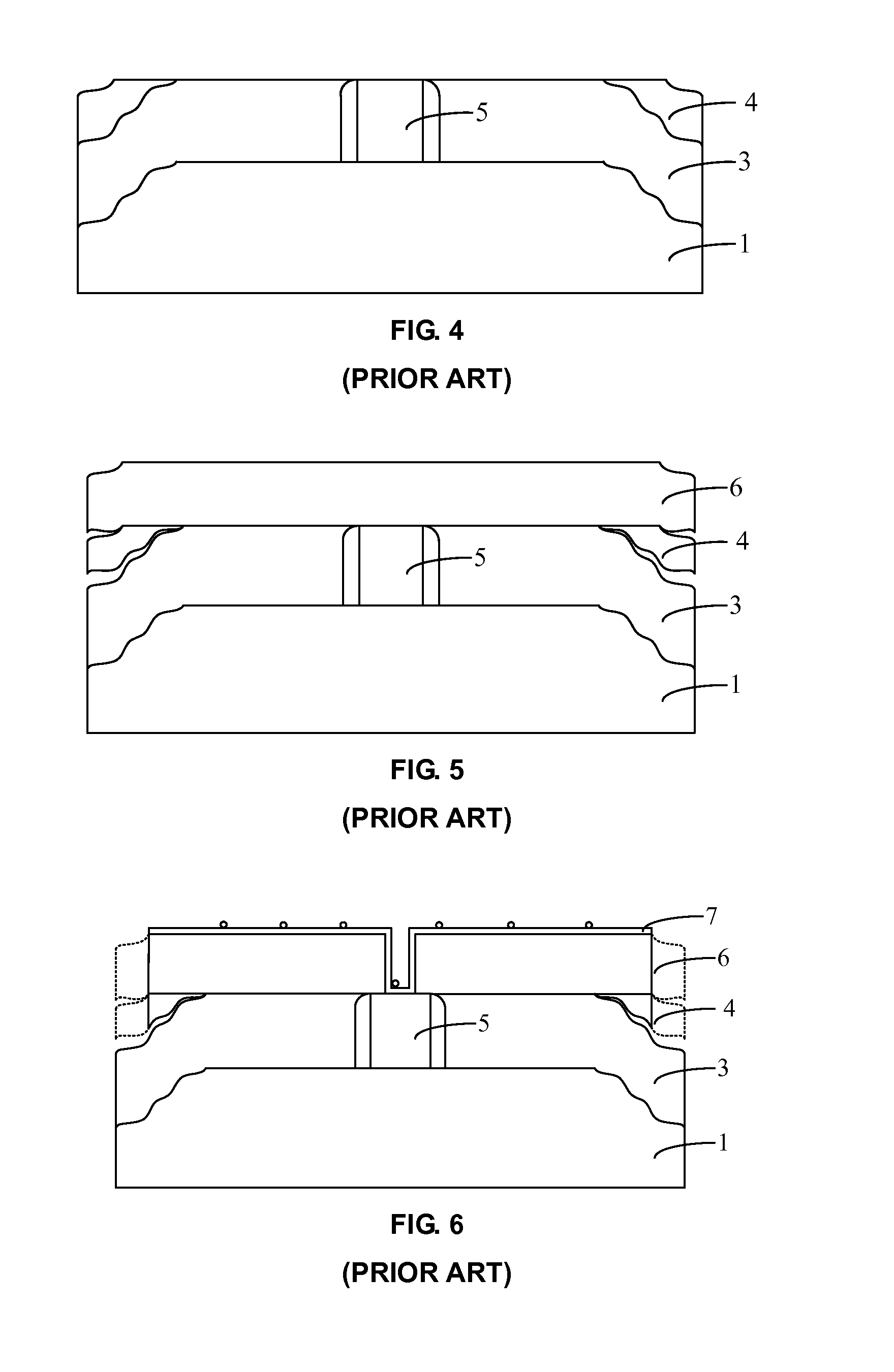
[0015]Reference will now be made in detail to exemplary embodiments of the disclosure, which are illustrated in the accompanying drawings. Wherever possible, the same reference numbers will be used throughout the drawings to refer to the same or like parts.
[0016]Metal gate transistors can suffer from poor performance because of the following reasons. Referring back to FIGS. 1-2, before a first interlayer dielectric layer 3 is formed on a top surface of a substrate 1, due to effects of various preceding semiconductor process steps, a top edge of the substrate 1 can be undesirably etched with edge defects. For example, the edge defects may provide an edge surface of the substrate 1 lower than a non-edge surface of the substrate 1. In other words, the edge defects may result in a ‘sunken edge’ or ‘lowered edge’ on the substrate. Thus, referring to FIG. 2, after the first interlayer dielectric layer 3 is formed, an edge portion (or edge) of the first interlayer dielectric layer 3 can ha...
PUM
 Abstract
Description
Claims
Application Information