Inductive energy supply unit

Inactive Publication Date: 2014-12-11
PHOENIX CONTACT GMBH & CO KG
13 Cites 12 Cited by

AI-Extracted Technical Summary

Problems solved by technology

Because of the ferromagnetic limbs, relatively free positioning between primary and secondary sides is not possible.
This results in potenti...

Benefits of technology

[0014]As is well known, a coil having helical turns produces magnetic flux lines which, inside the coil, extend parallel to the coil axis and bend outwards outside of the coil and turn round and run parallel or almost parallel to the coil axis in order to bend inward again towards the inside of the coil. Axially parallel flux lines stand perpendicular or almost perpendicular on planes spanned by the receiving coils so that effective coupling between transmitting coils and receiving coils takes place. If the receiving coils are accommodated on a circuit board, it is advantageous to let the turns extend spirally. Such coils can be produced in a cost-effective manner and have a large capture cross-section for flux lines.
[0015]Industrial installation...

Abstract

A device for supplying electrical energy and/or supplying data to an electronic module, comprising a transmitting coil that has a coil axis and at least two energy receiving parts that are arranged side by side and have receiving coils, the coil axes of which run in the same direction or run parallel to the transmitting coil axis. Each of the coils is integrated in resonance circuits. The energy receiving parts supply electronics and, together with the same, are galvanically separated from one another by an insulating area of separation which is bridged by a data signal coupling line.

Application Domain

Near-field transmissionBatteries circuit arrangements +6

Technology Topic

Supply energyElectric energy +10

Image

  • Inductive energy supply unit
  • Inductive energy supply unit
  • Inductive energy supply unit

Examples

  • Experimental program(1)

Example

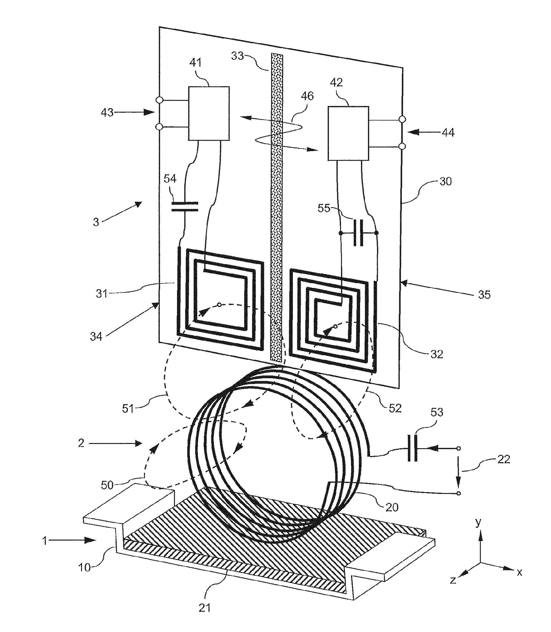
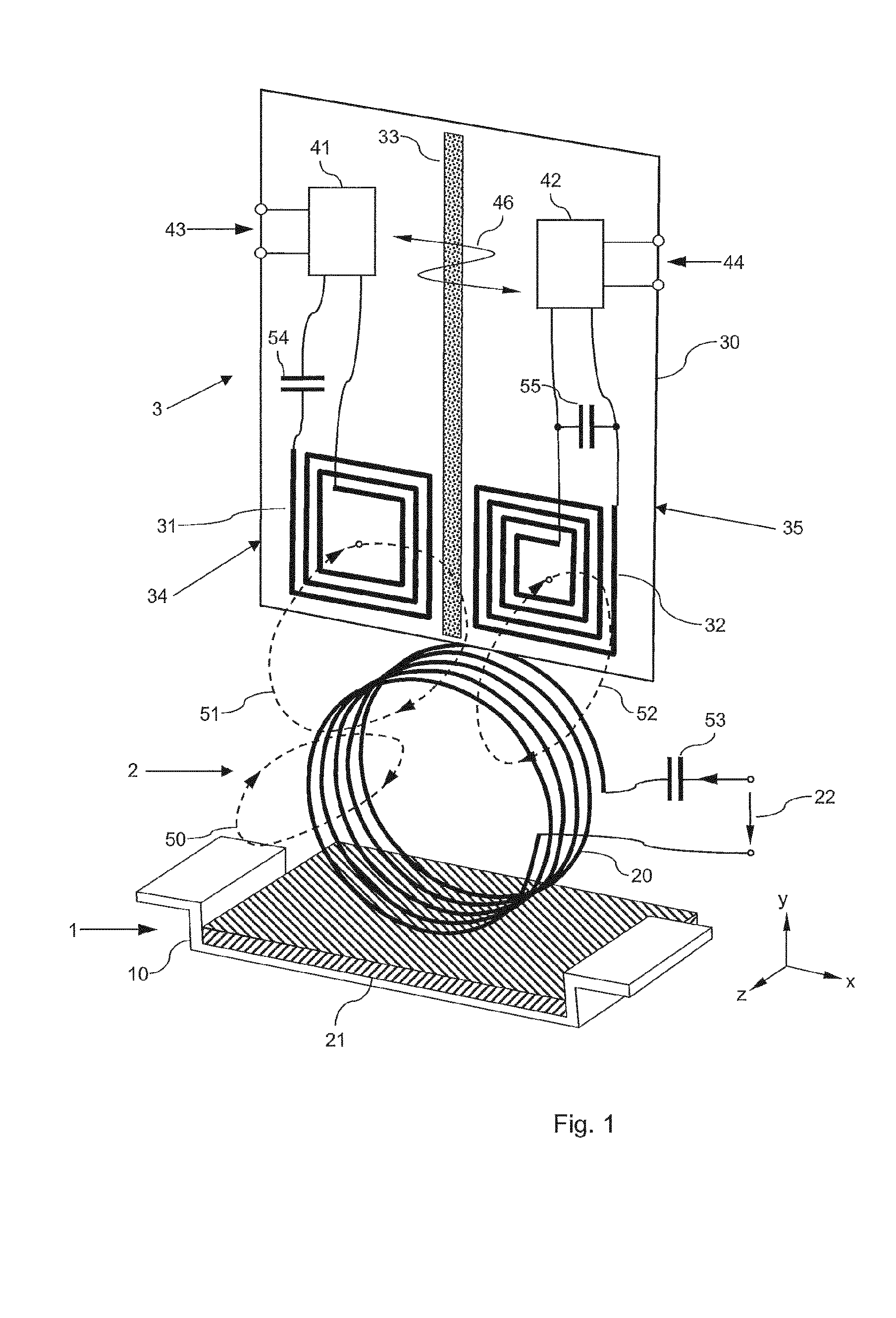
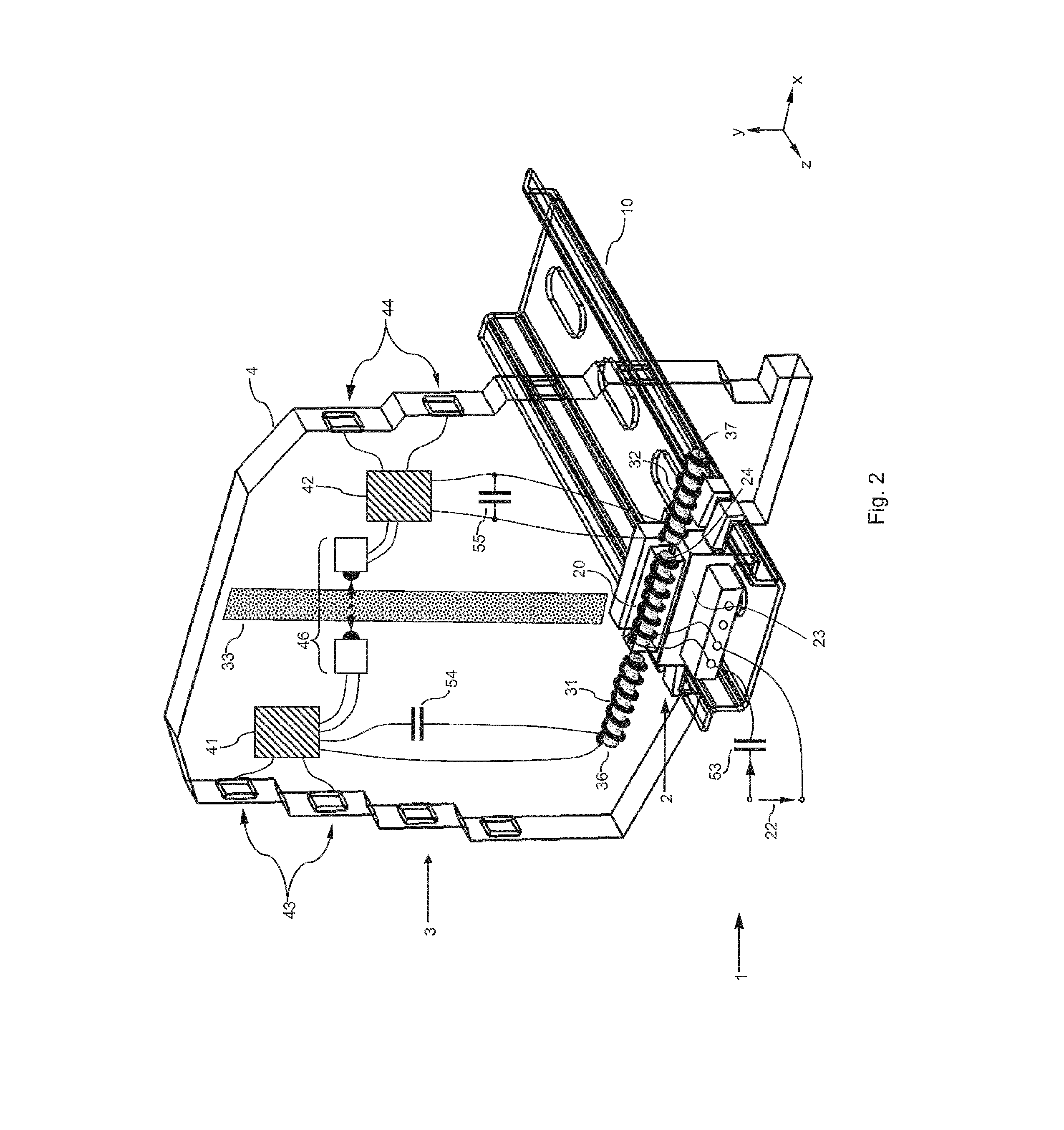
[0019]On a support rail 10 of an elongated module holding device 1, a transmitting coil 20 is secured which is supplied via an alternating input voltage 22 and thus acts as energy supply part 2. At a certain distance from the transmitting coil 20, a circuit board 30 is held by means of a housing 4 (FIG. 2) which is supported on the rail 10. Two spiral-shaped flat receiving coils 31, 32 which are separated from one another by an insulating area of separation 33 are fitted as conductor paths on the circuit board 30. The first receiving coil 31 is connected to a first electronics 41 and the second receiving coil 32 is connected to a second electronics 42. The components 31, 41, 54 form a first energy receiving part 34, and the components 32, 42, 55 form a second energy receiving part 35 of an electronic module 3.
[0020]The first electronics 41 can represent a signal or data input electronics and the second electronics 42 can be a signal or data output electronics of the electronic module 3. The two electronics 41, 42 are connected to one another via a data signal coupling line 46 in order to exchange data or signals between the electronics. The coupling line 46 can be formed by coupling elements which can represent an optical signal line; however, other transmission methods with capacitive or inductive coupling elements can also be used. As an alternative, the magnetic coupling between the coils 31 and 32 can also be utilized for signal or data transfer.
[0021]The transmitting coil 20 is helically wound and has a coil axis parallel to the longitudinal extent of the support rail 10. The receiving coils 31 and 32 are spirally wound and have coil axes that run parallel to one another and to the transmitting coil axis.
[0022]If the transmitting coil 20 is excited via the alternating supply voltage 22, an alternating magnetic field is created, of which some flux lines 50, 51,52 are outlined. The magnetic field portion illustrated by the flux line 51 passes through the flat receiving coil 31. Accordingly, the magnetic field portion illustrated by the flux line 52 passes through the flat receiving coil 32, while the flux line 50 represents the stray field. However, when the coil 20 is excited, capacitance effects act in addition to inductance between the coil turns, that is, the coil 20 as such already forms an electrical resonance circuit with a particular natural resonant frequency. The latter can be trimmed by means of one or more capacitors to a particular value which, for example, can correspond to the operating frequency of the input voltage. The capacitive influences of the vibratory system are symbolized by the total capacitance 53.
[0023]In practice, this capacitance can be formed by a series capacitor. Alternatively or additionally, a parallel capacitor can also be used. Finally, it is also possible to geometrically form the coil in such a manner that the operating frequency of the input voltage 22 corresponds to the natural resonant frequency of the coil 20 so that no discrete capacitor is needed, i.e., the total capacitance 53 is exclusively composed of the parasitic coupling capacitances of the coil turns.
[0024]If the coil 20 is excited, the coils 31 and 32 are also excited as a result of the inductive coupling. Here too, capacitance effects occur between the individual coil turns. For adapting to a common or almost common resonant frequency between the oscillating circuits with the coils 20, 31, 32, the capacitance effects between the individual coil turns can be specifically utilized, or capacitors in series connection or in parallel connection or in combination of these two circuit types are likewise utilized here so as to set a suitable capacitance 54, 55 by means of which the receiving circuits can be operated at resonant frequency.
[0025]In order to limit harmful effects of leakage inductance, shielding materials, for example from ferrite material, can be provided. Such a shielding plate 21 extends between transmitting coil 20 and rail 10. The receiving coils 31, 32 can also be shielded with respect to adjacent coils by ferrite material.
[0026]The insulating area of separation 33 can be created in that insulating material is located there which is not penetrated by conductor paths or other electronic components. The electronics 41, 42 as well as the signal terminals 43 and 44 can be attached on different sides of the circuit board 30. The electronic module 3 is secured in the housing 4 (FIG. 2) in such a manner that the signal terminals 43, 44 are accessible for plug connectors, for example.
[0027]The housing 4 is suited for being fastened as a plurality of identical housings arranged next to one another on a holding device 1, for example in the form of the rail 10, and thus to be arranged next to one another held in a row as a plurality of electronic modules 3 along the elongated holding device 1. Furthermore, a number of transmitting coils 20 which are aligned with one another and with which the electronic modules can be aligned extend along the holding device 1. The plurality of electronic modules 3 does not have to correspond to the number of transmitting coils 20. On the one hand, the electronic modules can be built particularly narrow; on the other, it is also possible to accommodate particularly wide electronic modules in the row of electronic modules. Overall, a system consisting of electrical energy supply and of a plurality of electronic modules can be created, in which increased insulation between separated potential groups is created.
[0028]FIG. 2 shows a second exemplary embodiment of the device for supplying electrical energy and supplying data to an electronic module 3. Parts identical to the exemplary embodiment 1 are designated by the same reference numbers. In addition, an appliance housing 4 is provided to protect the individual components of the electronic module 3 and to hold them in a defined arrangement with respect to the holding device 1.
[0029]The energy supply part 2 of the electronic module 3 has a base element 23 that partially protrudes into the housing 4 and is detachably connected to the elongated holding device 1. The base element 23 contains the transmitting coil 20, which is held well insulated with respect to its neighborhood by means of a plastic housing. The plastic housing is secured on the support rail 10 by latching. The transmitting coil 20 contains a ferrite core 24 which bundles the alternating magnetic field and directs it towards the coils 31. The coils 31 and 32 can also contain ferrite cores, as indicated at 36 and 37. The shape of the ferrite cores 36, 37 does not have to be rod-shaped; backward-bent shapes are also possible so as to keep magnetic reluctance low.
[0030]In FIG. 2, the coupling line 46 is indicated as optical insulating distance. Data between the two electronics 41 and 42 are thus transferred via the insulating area of separation 33. The increased safety requirements can also be managed via inductive, capacitive or electromagnetic transmission methods. Recesses keeping a safety distance between them are provided in the housing 4 for the signal connectors 43 and 44.
[0031]Data signals modulated on the energy signals can also be transmitted via the coil systems 20, 31, 32. The different safety standards can be met here as well.
[0032]The operation of the electronic modules takes place as follows: An operating frequency of the alternating supply voltage is selected in accordance with the resonant frequency of the oscillating circuits. The alternating supply voltage 22 drives current through the transmitting coil 20, as a result of which an alternating magnetic field is produced, symbolized by the flux lines 50, 51, 52. Due to the inductive coupling, respective alternating currents are produced in the receiving coils 31 and 32, which alternating currents, at resonance of the coils, enable operating the load with higher efficiency. In practice, said load typically consists of a rectifier circuit, a smoothing capacitor and the electronics 41, 42 connected thereto. The electronics can be integrated on the circuit board or can be accommodated externally. The energy of the source thus travels via the magnetic fields into the respective electronics 41 or 42 in order to be available there as energy source for signal and data processing. The magnetic field symbolized by the flux lines 50, 51 also includes an energy portion that, in a way, is collected or compensated by the capacitor 53. Therefore, ideally, only that amount of electrical energy is fed into the system that is consumed by the electronics 41 and 42. As viewed from the electrical voltage supply 22, the load formed by the electronics appears as purely ohmic load under ideal resonance conditions.
[0033]Similar to the transmitting coil where the inductance is almost compensated by the capacitance 53, the inductance in the case of the receiving coils 31, 32 is almost compensated by the capacitances 54 and 55. These are the positive effects of resonant circuits.
[0034]The illustrated exemplary embodiment can be modified in different ways. Thus, the two receiving coils can be attached on different sides of the circuit board, wherein in this case, the circuit board can serve as separation area.
[0035]Furthermore, it is possible to use the alternating input voltage 22 for energy supply as well as for data signal input. For this, the energy can be transmitted via a carrier signal and the data signal can be transmitted as modulation. In the receiving coils, the energy signal is then separated from the data signal. Thus, the transmitting coil together with in each case one of the receiving coils forms a data signal coupling line.
[0036]Data signal transmission can also take place from the receiving coils to the transmitting coil, namely by means of the so-called method of load modulation, for example. In the respective electronics, type and magnitude of the load is changed which has retroactive effects on the current/voltage ratio in the transmitting coil so that these retroactive effects can be detected as data signal on the transmitting side. In the case of this data signal coupling line, subcarriers can be used to better separate the energy signal from the data signal.
[0037]Data exchange between the receiving coils is also possible since they magnetically coupled to one another. By suitably adding additional capacitance, for example, a second resonant frequency can be generated which is used as a carrier for data signals.
[0038]Instead of two receiving coils, it is also possible to group a plurality of receiving coils around the transmitting coil so as to operate multi-channel systems. The modules can be arranged in two, three or four separate planes and can be galvanically separated from one another. The data signal coupling line between the electronics of the different planes can be of optical, magnetic or capacitive nature.

PUM

no PUM

Description & Claims & Application Information

We can also present the details of the Description, Claims and Application information to help users get a comprehensive understanding of the technical details of the patent, such as background art, summary of invention, brief description of drawings, description of embodiments, and other original content. On the other hand, users can also determine the specific scope of protection of the technology through the list of claims; as well as understand the changes in the life cycle of the technology with the presentation of the patent timeline. Login to view more.

Similar technology patents

Optical combiner device

ActiveUS20050175347A1cost-effectiveminimize loss
Owner:OMRON MANAGEMENT CENT OF AMERICA

Imposed current motor drive

Owner:DIALOG SEMICONDUCTOR

Structure of button for electronic product

InactiveUS6861603B1cost-effectiveeliminate jamming
Owner:PATEN WIRELESS TECH

Classification and recommendation of technical efficacy words

  • cost-effective

Nano graphene platelet-based conductive inks

InactiveUS20100000441A1cost-effectivelow viscosity
Owner:GLOBAL GRAPHENE GRP INC

Button anchor system for moving tissue

InactiveUS20060064125A1simple and easy to usecost-effective
Owner:CANICA DESIGN

Data stream filtering apparatus & method

InactiveUS20020146026A1cost-effectivesimple and low cost
Owner:RPX CLEARINGHOUSE
Why Eureka
Try Eureka