Semiconductor device and method for manufacturing semiconductor device

a semiconductor and semiconductor technology, applied in the direction of printed circuit aspects, high current circuit adaptations, basic electric elements, etc., can solve the problems of increasing capacity and reducing production efficiency, and achieve the effect of improving production efficiency

Active Publication Date: 2014-12-18
FUJI ELECTRIC CO LTD
View PDF2 Cites 41 Cited by
  • Summary
  • Abstract
  • Description
  • Claims
  • Application Information

AI Technical Summary

Benefits of technology

[0022]According to embodiments of the invention, it is possible to provide a semiconductor device and a semiconductor device manufacturing method which can perform modularization depending on current rating to improve production efficiency.

Problems solved by technology

In particular, it is a challenge to increase capacity or a breakdown voltage in the above-mentioned semiconductor module.
As a result, production efficiency is reduced.

Method used


Image

  • Semiconductor device and method for manufacturing semiconductor device
  • Semiconductor device and method for manufacturing semiconductor device
  • Semiconductor device and method for manufacturing semiconductor device

Examples


embodiment 1

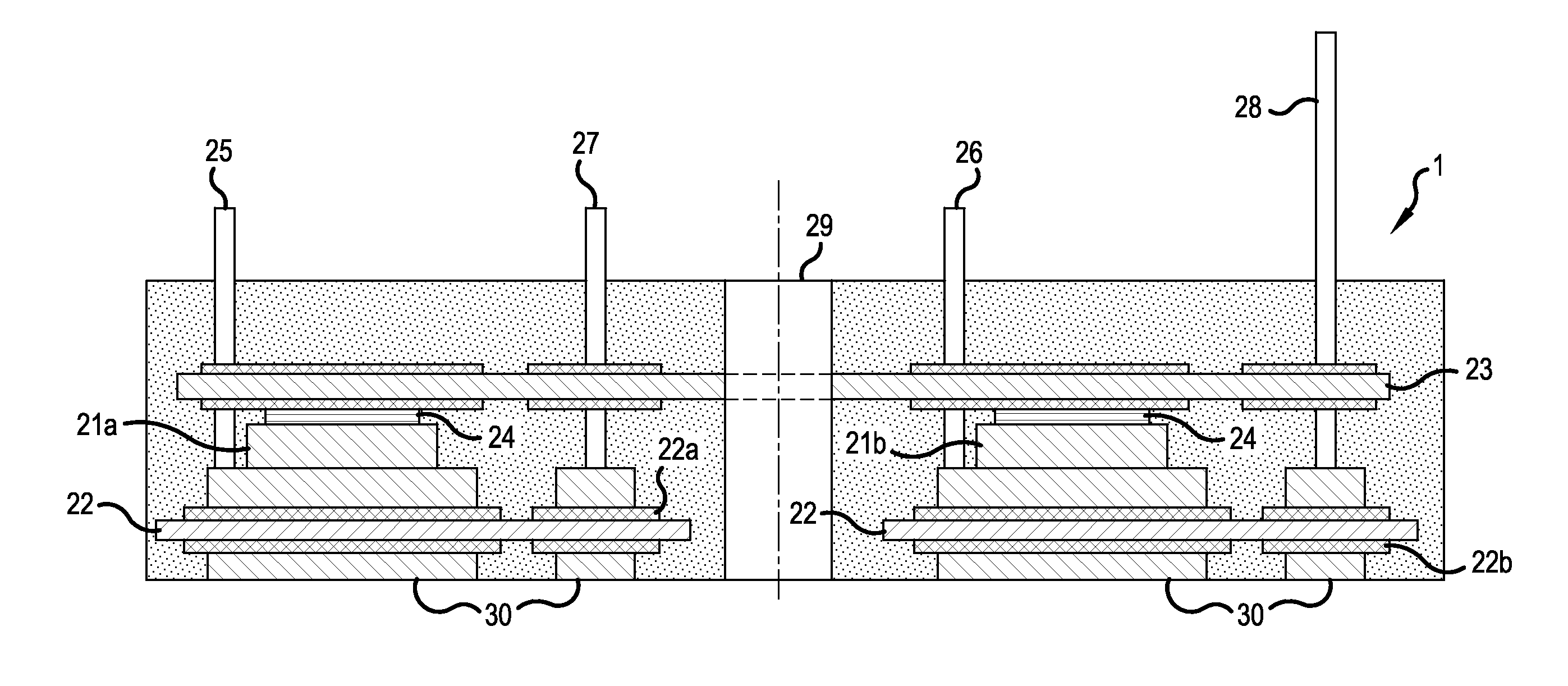
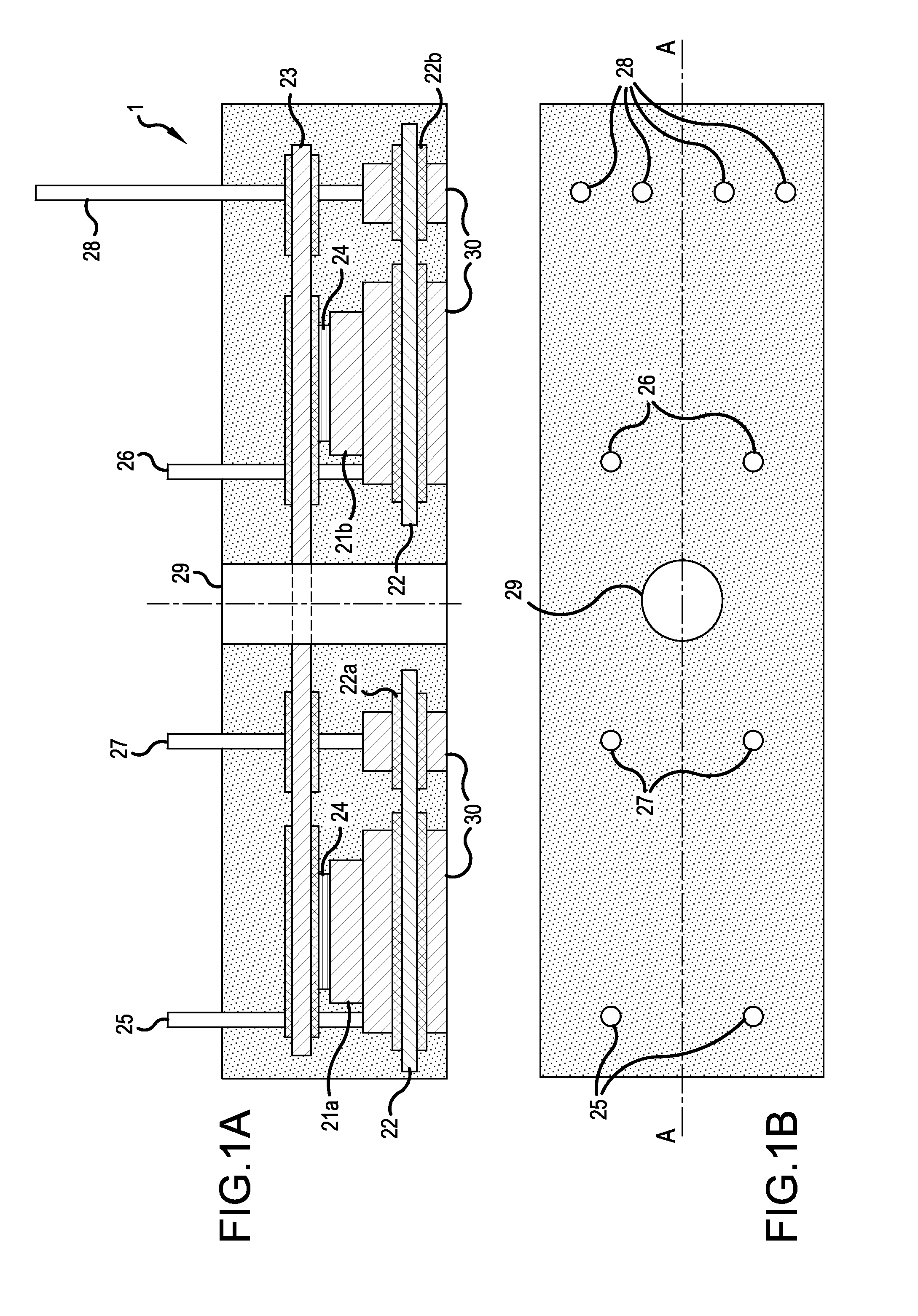
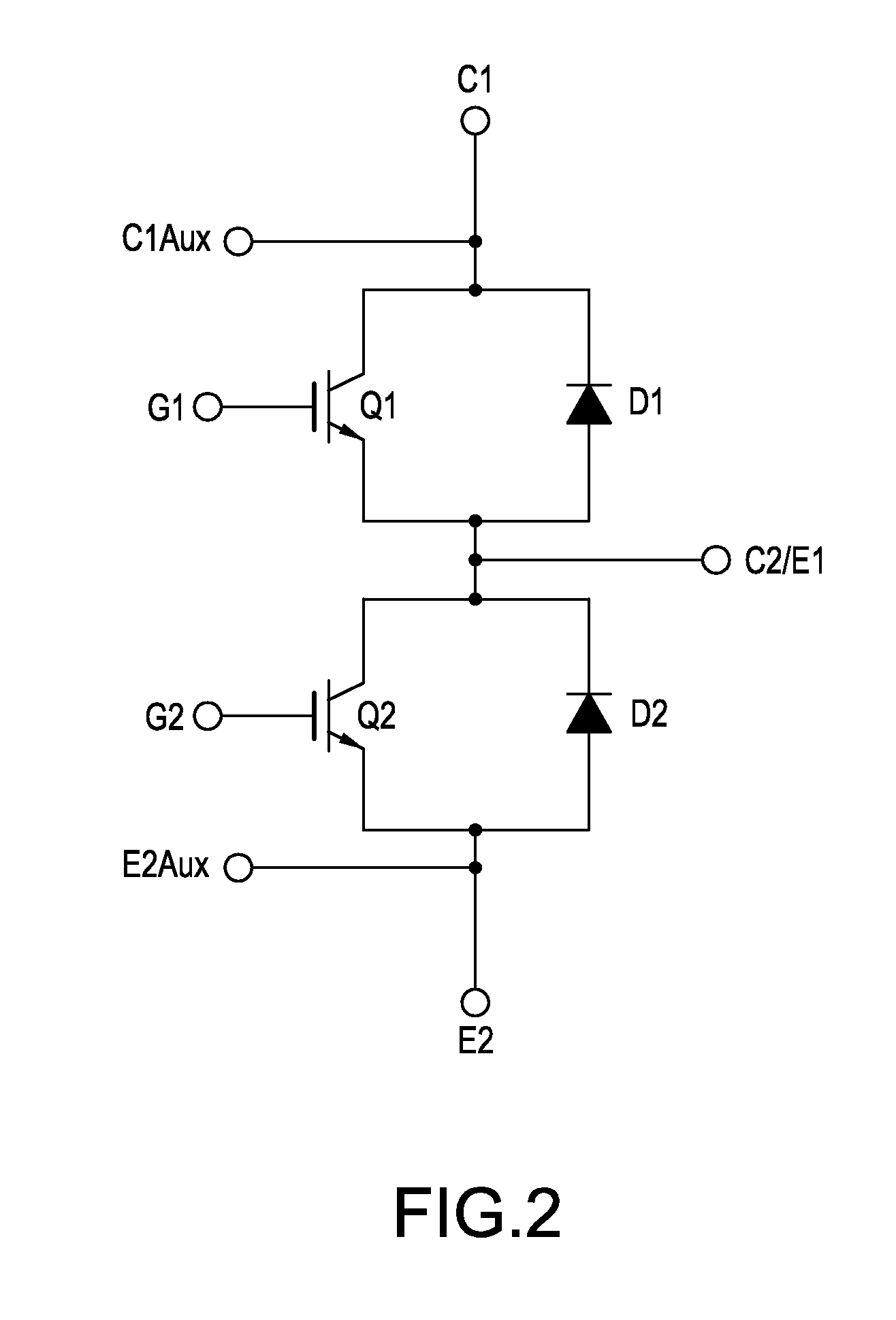
[0043]FIG. 1A is a cross-sectional view and FIG. 1B is a plan view illustrating a power semiconductor module according to a first embodiment of the invention. FIG. 2 is an equivalent circuit diagram illustrating a semiconductor circuit formed by the power semiconductor module illustrated in FIG. 1.

[0044]A power semiconductor module 1 includes two semiconductor circuits formed by mounting semiconductor chips 21a and 21b on insulating substrates 22 and a wiring substrate 23, which forms a common wiring circuit above the semiconductor circuits. In the semiconductor circuits, each of the semiconductor chips 21a and 21b is formed by a power device, such as an IGBT, a power metal-oxide-semiconductor field-effect transistor (MOSFET), or an FWD. For ease of understanding of illustration, only one semiconductor chip 21a (21b) is mounted on one insulating substrate 22 in FIG. 1. In practice, a switching device, such as an IGBT, and an FWD are provided on a conductor layer on the front surface...

embodiment 2

[0071]FIG. 7A is a cross-sectional view and FIG. 7B is a plan view illustrating a power semiconductor module according to a second embodiment.

[0072]A power semiconductor module 10 illustrated in FIG. 7 differs from the power semiconductor module 1 according to Embodiment 1 in that plate-shaped conductors 41 to 43 replace the pin-shaped conductors 25 to 27. The plate-shaped conductors 41 to 43 form an external input terminal (collector terminal C1), an external input terminal (emitter terminal E2), and an external output terminal (collector / emitter terminal C2 / E1), respectively, and have fastening opening portions 4h provided at the leading ends. That is, each component of the power semiconductor module 10 is molded by an epoxy resin material, which is a thermosetting resin, and the leading ends of the plate-shaped conductors 41 to 43 are bent at an angle of 90 degrees to form three terminal portions 44 to 46 each having the fastening opening portion 4h.

[0073]In Embodiment 2, the co...

embodiment 3

[0079]FIGS. 10A and 10B are diagrams illustrating a composite module according to a third embodiment. FIG. 10A is a diagram illustrating a semiconductor module before it is accommodated in a protective case and FIG. 10B is a diagram illustrating a state in which a main terminal segment is bent above the surface of the protective case.

[0080]In this embodiment, the composite module includes three power semiconductor modules 1A to 1C and main terminal plates 2B, 2C, and 2G (2GU, 2GV, and 2GW). Similarly to the power semiconductor module 1 according to Embodiment 1, each of the power semiconductor modules 1A to 1C includes pin-shaped conductors 25 to 27 serving as external input / output terminals and pin-shaped conductors 28 forming control (auxiliary) terminals (see FIG. 1). The third embodiment differs from Embodiment 1 in that independent main terminal segments 4G (4GU, 4GV, and 4GW) are drawn from the pin-shaped conductors (pin terminals) forming external input terminals (collector t...


PUM


Abstract

A semiconductor device is a composite module in which three power semiconductor modules are arranged at a predetermined interval in the same plane and pin-shaped conductors that are drawn from the power semiconductor modules to the outside are connected to three main terminal plates such that they are integrated with each other. When the entire composite module is accommodated in a protective case and a radiation fin is provided, bolts are inserted into through holes to fix the protective case to the radiation fin. In this way, it is possible to accommodate the composite module in the protective case while reliably bringing the bottom of an insulating substrate into close contact with the radiation fin.

Description

CROSS REFERENCE TO RELATED APPLICATIONS[0001]This application is a continuation of International Application No. PCT / JP2013 / 056634, filed on Mar. 11, 2013, which is based on and claims priority to Japanese Patent Application No. JP 2012-072673, filed on Mar. 28, 2012. The disclosure of the Japanese priority application and the PCT application in their entirety, including the drawings, claims, and the specification thereof, are incorporated herein by reference.BACKGROUND[0002]1. Field of the Invention[0003]Embodiments of the present invention relate to a semiconductor device that includes a semiconductor module including, for example, a power device and has a common external connection structure and a method for manufacturing a semiconductor device.[0004]2. Discussion of the Background[0005]A power inverter device has been widely used as one of power conversion devices. For example, a motor is generally used as a driving source of an electric vehicle and the inverter device is genera...

Claims


Application Information

Patent Timeline
Patent Type & Authority Applications(United States)
IPC IPC(8): H01L23/00H01L29/66H01L23/34
CPCH01L24/80H01L24/02H01L23/34H01L2924/01082H01L2224/06H01L2924/0105H01L2924/01028H01L29/66325H01L25/18H01L2224/48091H01L2224/48227H01L2224/45124H05K1/0263H05K2201/10166H02M7/003H01L25/072H01L23/3107H01L23/5385H01L2924/13091H01L2924/13055H01L2924/12032H01L2924/1305H01L23/49811H01L2924/01322H01L2924/15787H01L23/051H01L2924/181H01L2924/12042H01L25/115H01L2924/00014H01L2924/00H01L2924/00012H01L25/117
Inventor IIZUKA, YUJIHORIO, MASAFUMINAKAMURA, HIDEYO
Owner FUJI ELECTRIC CO LTD
Why Eureka
Try Eureka