Light emitting diode structure

a technology of light-emitting diodes and diodes, which is applied in the direction of basic electric elements, electrical apparatus, and semiconductor devices, can solve the problems of increasing manufacturing costs and unable to enhance the light-emitting efficiency of light-emitting diodes, and achieves the effects of improving light-emitting diodes, reducing manufacturing costs, and improving light-emitting diodes

Active Publication Date: 2014-12-25
LEXTAR ELECTRONICS CORP
View PDF0 Cites 2 Cited by
  • Summary
  • Abstract
  • Description
  • Claims
  • Application Information

AI Technical Summary

Benefits of technology

The present invention provides a light emitting diode structure with a reverse current protection element that can be manufactured at the same time as the LED element, reducing manufacturing costs and not taking up module space. The reverse current protection element includes a stack layer formed on the substrate by sequentially stacking layers of different conductivity, and an insulation gap between the reverse current protection element and the LED element improves light efficiency and brightness.

Problems solved by technology

Thus, manufacturing costs are increased.
Moreover, a Zener diode takes up a module space for receiving the light emitting diode structure 200 and cannot enhance the light emitting efficiency of the light emitting diode structure 200.

Method used


Image

  • Light emitting diode structure
  • Light emitting diode structure
  • Light emitting diode structure

Examples


Embodiment Construction

[0037]Reference will now be made in detail to the present embodiments of the invention, examples of which are illustrated in the accompanying drawings. Wherever possible, the same reference numbers are used in the drawings and the description to refer to the same or like parts.

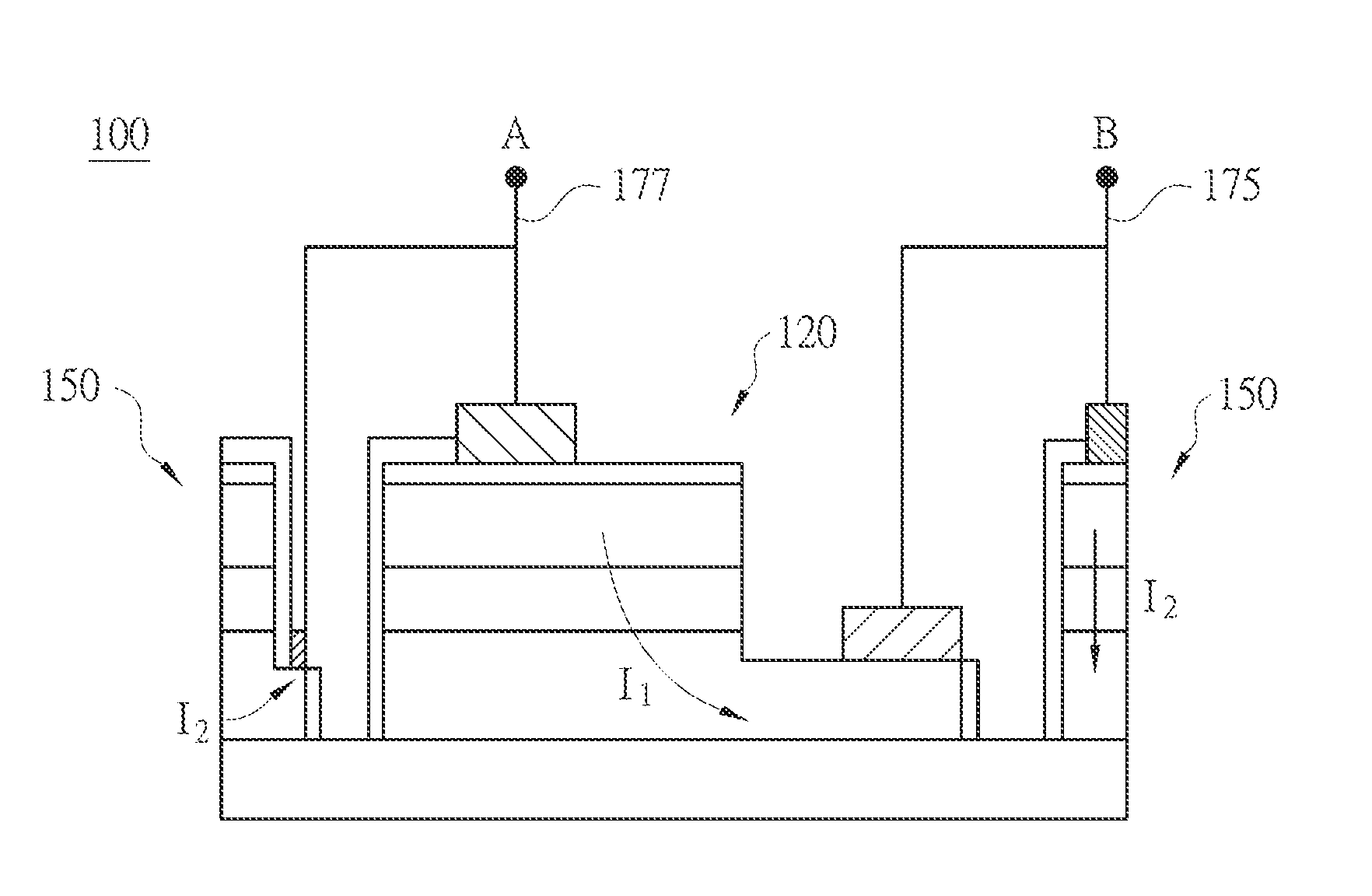
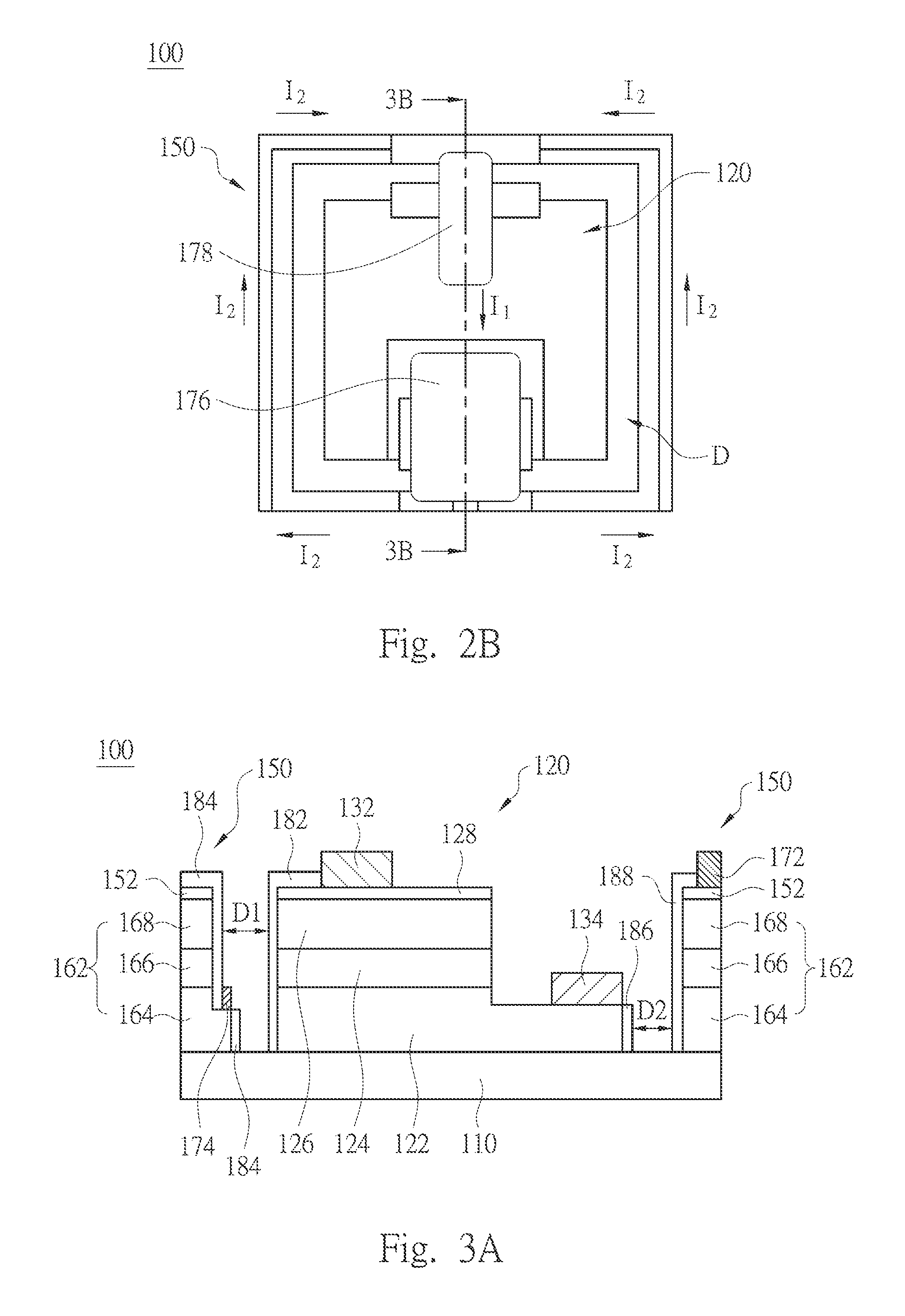
[0038]FIG. 2A is a top view of a light emitting diode structure 100 according to one embodiment of this invention. FIG. 2B is a top view of the light emitting diode structure 100 of FIG. 2A according to one embodiment of this invention, in which the light emitting diode structure 100 includes a third conductor 176 and a fourth conductor 178. Referring to FIGS. 2A and 2B, the light emitting diode structure 100 includes a substrate 110, an LED element 120, a reverse current protection element 150, the third conductor 176, and the fourth conductor 178. The reverse current protection element 150 is located on the substrate 110 and surrounds the LED element 120. Moreover, an insulation gap D is defined between the ...


PUM


Abstract

A light emitting diode (LED) structure includes a substrate, an LED element, a reverse current protection element, a third conductor, and a fourth conductor. The LED element includes a first N-type semiconductor layer, a first lighting layer, a first P-type semiconductor layer, a first transparent conductive layer, a first electrode, and a second electrode. The reverse current protection element is located on the substrate and surrounds the LED element. The reverse current protection element includes a stack layer, a first conductor, and a second conductor. The stack layer is formed on the substrate by sequentially stacking a second N-type semiconductor layer, a second lighting layer, and a second P-type semiconductor layer. The third conductor is electrically connected to the first conductor and the second electrode. The fourth conductor is electrically connected to the second conductor and the first electrode.

Description

RELATED APPLICATIONS[0001]This application claims priority to Taiwan Application Serial Number 102122193, filed Jun. 21, 2013, which is herein incorporated by reference.BACKGROUND[0002]1. Field of Invention[0003]The present invention relates to a light emitting diode structure.[0004]2. Description of Related Art[0005]FIG. 1 is a cross-sectional view of a conventional light emitting diode structure 200. As shown in FIG. 1, the light emitting diode structure 200 includes a substrate 210, and an N-type semiconductor layer 220, a light emitting layer 230, a P-type semiconductor layer 240, a transparent conductor layer 250, a positive electrode 260 and a negative electrode 270 are stacked on the substrate 210. Part of the N-type semiconductor layer 220 that is not covered by the light emitting layer 230, the P-type semiconductor layer 240, and the transparent conductor layer 250 may be formed by photolithography and etching processes. When the positive electrode 260 and the negative elec...

Claims


Application Information

Patent Timeline
Patent Type & Authority Applications(United States)
IPC IPC(8): H01L27/15
CPCH01L27/15
Inventor LAN, CHENG-CHUNCHOU, TZU-HUNGCHAO, CHI-CHUNG
Owner LEXTAR ELECTRONICS CORP
Why Eureka
Try Eureka