Mosfet with integrated schottky diode

a schottky diode and mosfet technology, applied in the direction of diodes, semiconductor devices, electrical apparatus, etc., can solve the problems of affecting the device performance, the use of schottky diodes in parallel with the mosfet device does have some drawbacks, and the limited switching frequency of the mosfet devi

Active Publication Date: 2014-12-25
ALPHA & OMEGA SEMICON INC
View PDF4 Cites 13 Cited by
  • Summary
  • Abstract
  • Description
  • Claims
  • Application Information

AI Technical Summary

Benefits of technology

[0004]However, the use of a Schottky diode in parallel with the MOSFET devices does have some drawbacks. First, Schottky diodes typically have high reverse bias current leakage which adversely affects the performance of the device. Additionally, the integration of a Schottky diode into an MOSFET device utilizes valuable space on the die that could otherwise be used for additional active devices. Further, the integration of a Schottky diode may increase the cost of manufacturing the MOSFET devices because additional mask sets may be needed to form the Schottky diode. Therefore, there is a need in the art for a Schottky diode that has minimal leakage and can be integrated into the device in a space conscious manner without needing additional masks.

Problems solved by technology

The switching frequency of MOSFET devices are limited by device characteristics, largely capacitances, and in the case of certain applications, namely DC-DC converters, the recovery of the parasitic diode inherent in all power MOSFET device structures.
However, the use of a Schottky diode in parallel with the MOSFET devices does have some drawbacks.
First, Schottky diodes typically have high reverse bias current leakage which adversely affects the performance of the device.
Additionally, the integration of a Schottky diode into an MOSFET device utilizes valuable space on the die that could otherwise be used for additional active devices.
Further, the integration of a Schottky diode may increase the cost of manufacturing the MOSFET devices because additional mask sets may be needed to form the Schottky diode.

Method used


Image

  • Mosfet with integrated schottky diode
  • Mosfet with integrated schottky diode
  • Mosfet with integrated schottky diode

Examples


Embodiment Construction

[0020]Although the following detailed description contains many specific details for the purposes of illustration, anyone of ordinary skill in the art will appreciate that many variations and alterations to the following details are within the scope of the invention. Accordingly, the exemplary embodiments of the invention described below are set forth without any loss of generality to, and without imposing limitations upon, the claimed invention.

[0021]In the following Detailed Description, reference is made to the accompanying drawings, which form a part hereof, and in which is shown by way of illustration specific embodiments in which the invention may be practiced. In this regard, directional terminology, such as “top,”“bottom,”“front,”“back,”“leading,”“trailing,”“first,”“second,” etc., is used with reference to the orientation of the figure(s) being described. Because components of embodiments of the present invention can be positioned in a number of different orientations, the d...


PUM


Abstract

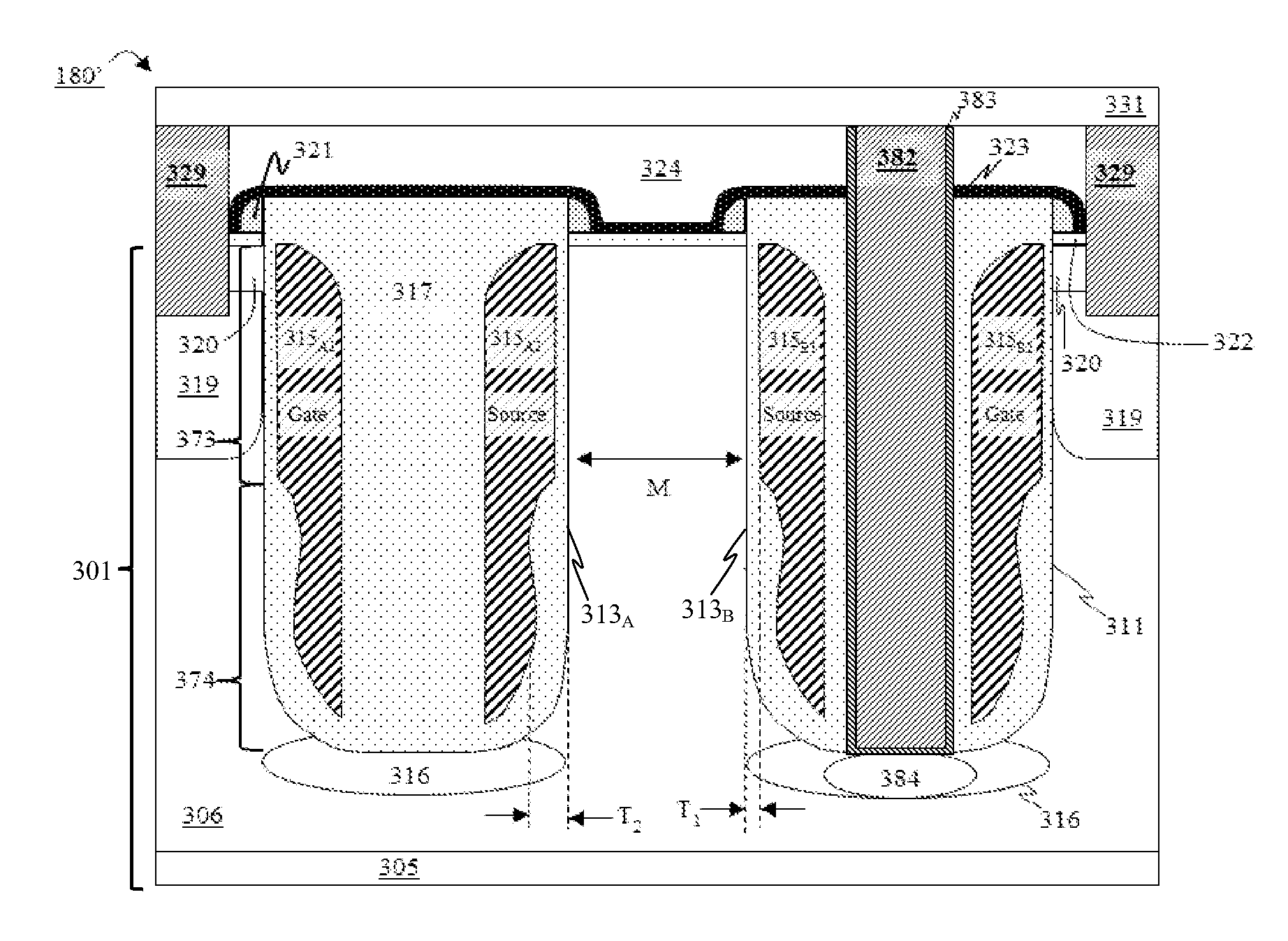
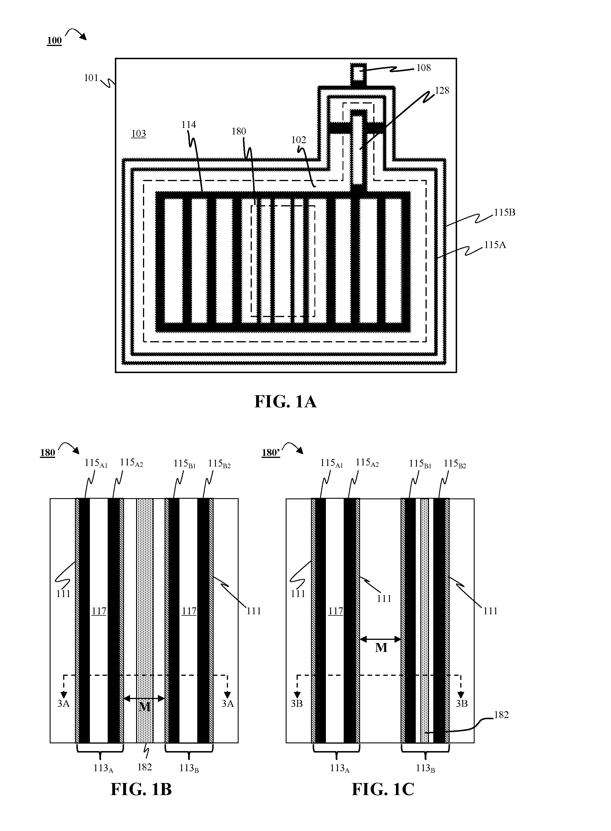
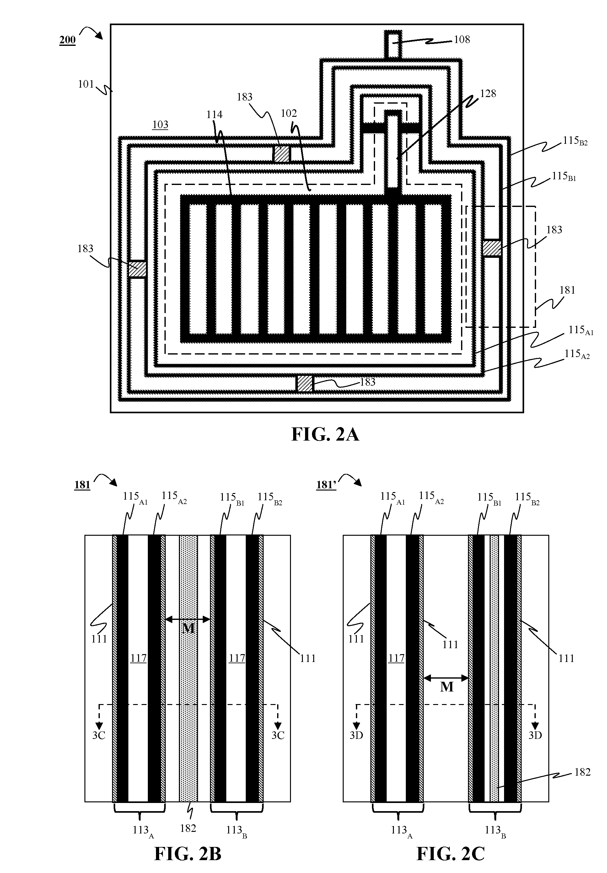
Aspects of the present disclosure describe a Schottky structure with two trenches formed in a semiconductor material. The trenches are spaced apart from each other by a mesa. Each trench may have first and second conductive portions lining the first and second sidewalls. The first and second portions of conductive material are electrically isolated from each other in each trench. The Schottky contact may be formed at any location between the outermost conductive portions. The Schottky structure may be formed in the active area or the termination area of a device die. It is emphasized that this abstract is provided to comply with rules requiring an abstract that will allow a searcher or other reader to quickly ascertain the subject matter of the technical disclosure. It is submitted with the understanding that it will not be used to interpret or limit the scope or meaning of the claims.

Description

CROSS-REFERENCE TO RELATED APPLICATION[0001]This application is related to commonly-assigned, co-pending application Ser. No. 13 / 776,523, (Attorney Docket Number ANO-061 / US) filed Feb. 25, 2013, and entitled “TERMINATION TRENCH FOR POWER MOSFET APPLICATIONS”, the entire disclosures of which are incorporated herein by reference.FIELD OF THE INVENTION[0002]This invention generally relates to power device structures and a method for manufacturing the device thereof. Specifically, the invention is directed to a method to implement an integrated Schottky diode into system that can include both active and passive devices and all the devices made from the method.BACKGROUND OF THE INVENTION[0003]Metal-oxide-semiconductor field-effect transistors (MOSFETs) are used for amplifying or switching electronic signals. A MOSFET device used for power switching is sometimes referred to as a power MOSFET. Power MOSFET devices typically contain multiple individual MOSFET structures arranged in active c...

Claims


Application Information

Patent Timeline
Patent Type & Authority Applications(United States)
IPC IPC(8): H01L27/06
CPCH01L27/0629H01L29/407H01L29/66719H01L29/66727H01L29/66734H01L29/7806H01L29/7808H01L29/7811H01L29/7813H01L29/0623H01L29/42368H01L29/41766H01L27/088H01L29/0619H01L29/66712H01L27/0251H01L21/823487H01L21/823475H01L21/308H01L29/1095H01L29/66143H01L29/7827H01L29/872H01L21/265H01L27/095H01L29/66257
Inventor CALAFUT, DANIELLEE, YEEHENG
Owner ALPHA & OMEGA SEMICON INC
Why Eureka
Try Eureka