
Isolation structure in gallium nitride devices and integrated circuits

a technology of gallium nitride and integrated circuit, which is applied in the direction of semiconductor devices, basic electric elements, electrical apparatus, etc., can solve the problems of etching surface with high leakage current, preventing the ic from functioning properly, and increasing the cos

Active Publication Date: 2015-01-08
EFFICIENT POWER CONVERSION CORP
View PDF8 Cites 5 Cited by
  • Summary
  • Abstract
  • Description
  • Claims
  • Application Information

AI Technical Summary

Benefits of technology

The patent text describes a manufacturing method for GaN semiconductor devices that includes an isolation region between two or more transistor devices. The method includes forming a substrate layer, a buffer layer, a gallium nitride layer, and a barrier layer. Ohmic contacts for a plurality of transistor devices are formed on the barrier layer, and one or more gate structures are formed on a portion of the barrier layer to electrically isolate the first transistor device from the second transistor device. The technical effect of this method is that it allows for the efficient production of integrated semiconductor devices with improved performance and reliability.

Problems solved by technology

Such devices could interfere with each other if not electrically isolated, preventing the ICs from functioning properly.
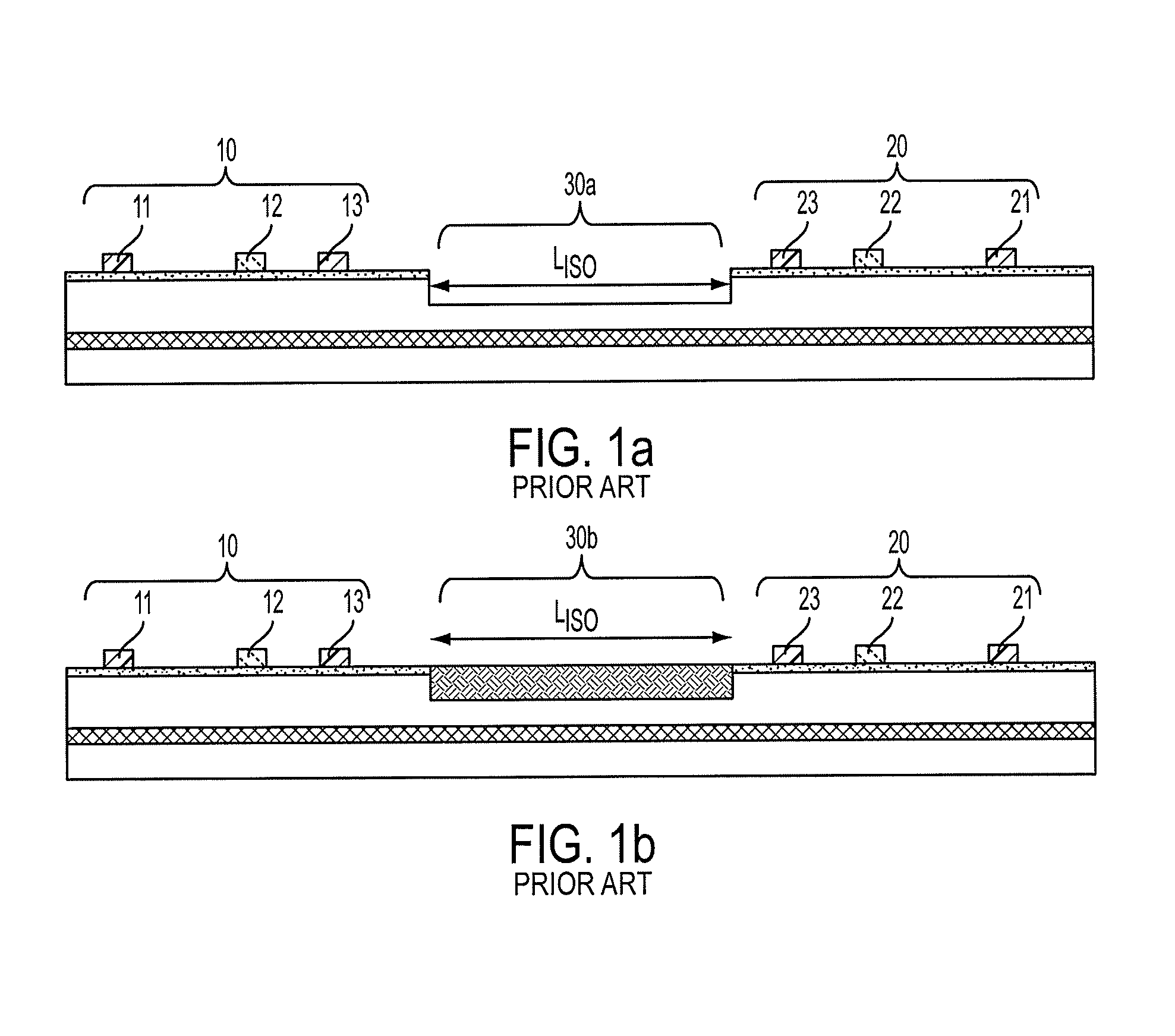
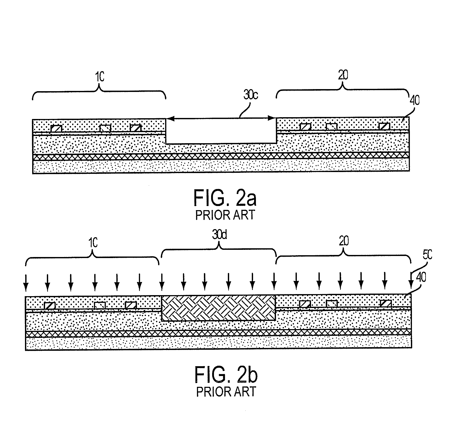
The existing methods of fabricating an isolation structure suffers from a number of disadvantages, including: (1) requiring a dedicated mask with the associated process steps that increase cost; (2) isolation by etching, which can result in an etched surface with high leakage current; and (3) isolation by ion-implantation in which the resistivity of the isolation region can degrade after the high temperature process.

Method used


Image

  • Isolation structure in gallium nitride devices and integrated circuits
  • Isolation structure in gallium nitride devices and integrated circuits
  • Isolation structure in gallium nitride devices and integrated circuits

Examples


first embodiment

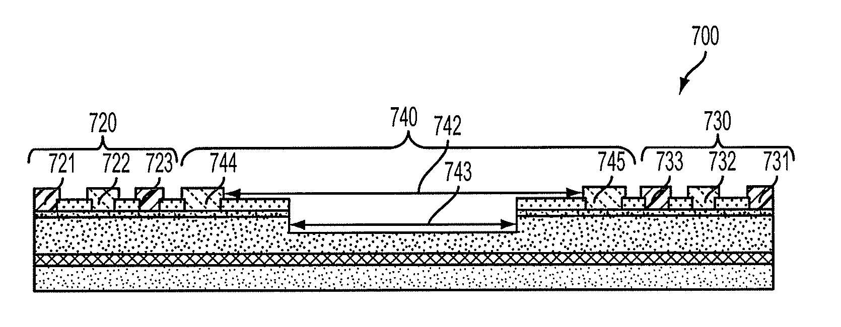
[0028]FIG. 3 illustrates a gallium nitride (GaN) semiconductor device 300 with an isolation structure 340 according to the present invention. The integrated semiconductor device 300 is formed on a substrate 311 that may comprise silicon (Si), silicon carbide (SiC) or sapphire, for example. A buffer layer 312 is formed on the substrate layer 311 and separates the substrate layer 311 from a gallium nitride (GaN) layer 313. In the exemplary embodiment, the gallium nitride (GaN) layer 313 is typically un-doped and has a thickness of 0.5 to 10 μm. A barrier layer 314 is formed over and in contact with the gallium nitride (GaN) layer 313. Further, the barrier layer 314 is formed of AlGaN and is typically un-doped and has a thickness of 50 Å to 300 Å with an aluminum (Al) composition from 10% to 35%.

[0029]The integrated semiconductor device 300 includes devices 320 and 330, which includes ohmic contacts 321 and 331 that form the drains of the devices. Ohmic contacts 323 and 333 form the so...

second embodiment

[0032]FIG. 4 illustrates a gallium nitride (GaN) semiconductor device 400 with an isolation structure 440 according to the present invention. The integrated semiconductor device 400 is formed on a substrate 411 that may comprise, for example, silicon (Si), silicon carbide (SiC) or sapphire. A buffer layer 412 is formed over the substrate layer 411 and separates the substrate layer 411 from the gallium nitride (GaN) layer 413, which is formed over buffer layer 412. Preferably, the gallium nitride (GaN) layer 413 is typically un-doped and has a thickness of 0.5 to 10 μm. A barrier layer 414 is formed over and in contact with the gallium nitride (GaN) layer 413. In the exemplary embodiment, barrier layer 414 is formed of AlGaN and is typically un-doped with a thickness of 50 Å to 300 Å and with aluminum (Al) composition from 10% to 35%.

[0033]Semiconductor device 400 includes devices 420 and 430. Ohmic contacts 421, 431 form the drains of devices 420 and 430 and ohmic contacts 423 and 4...

third embodiment

[0036]FIG. 5 illustrates a gallium nitride (GaN) semiconductor device 500 with an isolation structure 540 according to the present invention. In the exemplary embodiment, the integrated semiconductor device 500 is formed on a substrate 511 that may comprise, for example, silicon (Si), silicon carbide (SiC) or sapphire. A buffer layer 512 is formed on substrate 511 and separates the substrate layer 511 from the gallium nitride (GaN) layer 513 formed on the buffer layer 512. The gallium nitride (GaN) layer 513 is typically un-doped and has a thickness of 0.5 to 10 μm. A barrier layer 514 is formed over and in contact with the gallium nitride (GaN) layer 513. Barrier layer 514 is formed of AlGaN and is typically un-doped and has a thickness of 50 Å to 300 Å. Preferably, barrier layer 514 has an aluminum (Al) composition from 10% to 35%.

[0037]Devices 520 and 530 have drains contacts 521 and 531, sources contacts 523 and 533, gates 522 and 532 disposed between the respective drains 521, ...


PUM


Abstract

An integrated semiconductor device which includes a substrate layer, a buffer layer formed on the substrate layer, a gallium nitride layer formed on the buffer layer, and a barrier layer formed on the gallium nitride layer. Ohmic contacts for a plurality of transistor devices are formed on the barrier layer. Specifically, a plurality of first ohmic contacts for the first transistor device are formed on a first portion of the surface of the barrier layer, and a plurality of second ohmic contacts for the second transistor device are formed on a second portion of the surface of the barrier layer. In addition, one or more gate structures formed on a third portion of the surface of the barrier between the first and second transistor devices. Preferably, the one or more gate structures and the spaces between the gate structures and the source contacts of the transistor devices collectively form an isolation region that electrically isolates the first transistor device from the second transistor device.

Description

CROSS REFERENCE TO RELATED APPLICATIONS[0001]This application claims the benefit of U.S. Provisional Application No. 61 / 843,810, filed on Jul. 8, 2013, the entire disclosure of which is hereby incorporated by reference.BACKGROUND OF THE INVENTION[0002]1. Field of Invention[0003]The present invention relates to the field of gallium nitride (GaN) devices and integrated circuits. In particular, the invention relates to a structure and method for isolating electrical devices in an integrated semiconductor device.[0004]2. Description of the Related Art[0005]Gallium nitride (GaN) semiconductor devices are increasingly desirable because of their ability to switch at high frequency, to carry large current, and to support high voltages. Development of these devices has generally been aimed at high power / high frequency applications. Devices fabricated for these types of applications are based on general device structures that exhibit high electron mobility and are referred to variously as het...

Claims


Application Information

Patent Timeline
IPC IPC(8): H01L29/20H01L29/267H01L29/778
CPCH01L29/2003H01L29/267H01L29/778H01L21/76H01L27/0605H01L29/66462H01L29/7786
Inventor ZHOU, CHUNHUACAO, JIANJUNLIDOW, ALEXANDERBEACH, ROBERTNAKATA, ALANASTRITTMATTER, ROBERTZHAO, GUANG YUANKOLLURI, SESHADRIMA, YANPINGCHANG, FANGCHIANG, MING-KUNCAO, JIALI
Owner EFFICIENT POWER CONVERSION CORP
Learn More