Non-intrusive monitoring and control of integrated circuits

Active Publication Date: 2015-01-08
ALTERA CORP
View PDF2 Cites 49 Cited by
  • Summary
  • Abstract
  • Description
  • Claims
  • Application Information

AI Technical Summary

Benefits of technology

[0007]Some embodiments provide a system and method for obtaining visibility into an in-the-field device. These embodiments provide a monitoring tool that allows unobtrusive full read access to a running user design to enable rapid-response monitoring, debugging, and response to exceptions and other events.

Problems solved by technology

However, user signals as originally expressed in the RTL source code m

Method used


Image

  • Non-intrusive monitoring and control of integrated circuits
  • Non-intrusive monitoring and control of integrated circuits
  • Non-intrusive monitoring and control of integrated circuits

Examples


Embodiment Construction

[0057]In the following detailed description of the invention, numerous details, examples, and embodiments of the invention are set forth and described. However, it will be clear and apparent to one skilled in the art that the invention is not limited to the embodiments set forth and that the invention may be practiced without some of the specific details and examples discussed.

I. TERMS AND DEFINITIONS

[0058]A. Integrated Circuits (ICs)

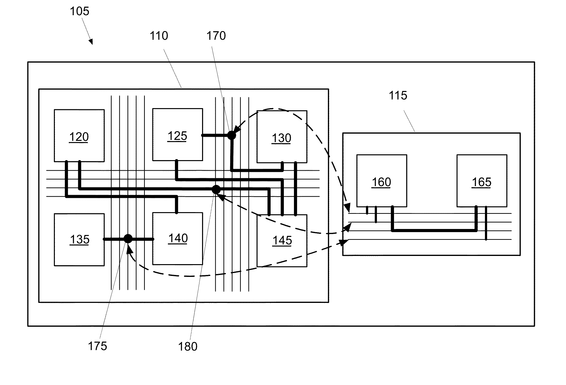
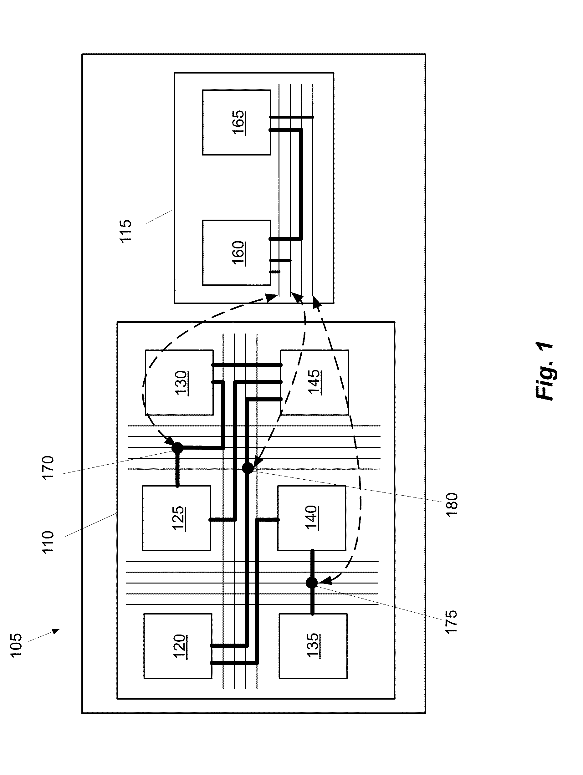
[0059]Some embodiments of the invention monitor and control the operations of an IC. An IC is a device that includes numerous electronic components (e.g., transistors, resistors, capacitors, diodes, etc.) that are typically embedded on the same substrate, such as a single piece of semiconductor wafer. These components are connected with one or more layers of wiring to form multiple circuits, such as Boolean gates, memory cells, arithmetic units, controllers, decoders, etc. An IC is often packaged as one chip in a single IC package, although some IC pack...


PUM


Abstract

A method of monitoring operations of a set of ICs. The method loads a first set of configuration data into a first IC for configuring a group of configurable circuits of the first IC to perform operations of a user design. The method receives a definition of an event based on values of a set of signals in the user design and a set of corresponding actions to take when the event occurs. The set of signals includes at least one signal received from a second IC. The method generates an incremental second set of configuration data based on the definition of the event and the set of corresponding actions. While the first IC is performing the operations of the user design, the method loads the incremental second set of configuration data into the first IC and monitors the signals received from the second IC at the first IC.

Description

CLAIM OF BENEFIT TO PRIOR APPLICATIONS[0001]The present application claims the benefit of U.S. Provisional Patent Application 61 / 842,966, entitled, “Non-Intrusive Monitoring and Control of Integrated Circuits,” filed Jul. 4, 2013; U.S. Provisional Patent Application 61 / 843,921, entitled, “Non-Intrusive Monitoring and Control of Integrated Circuits,” filed Jul. 9, 2013; and U.S. Provisional Patent Application 61 / 879,578, entitled, “Non-Intrusive Monitoring and Control of Integrated Circuits,” filed Sep. 18, 2013. The contents of U.S. Provisional applications 61 / 842,966, 61 / 843,921, and 61 / 879,578 are hereby incorporated by reference.BACKGROUND[0002]Programmable Logic Devices (“PLDs”) are configurable integrated circuits (“ICs”) which can be used to implement multiple circuit designs created by users (“user designs”) without having to fabricate a new IC for each design. However, due to the complexity of the systems being implemented, such user designs usually include various design bu...

Claims


Application Information

Patent Timeline
IPC IPC(8): H03K19/177G01R31/26
CPCG01R31/2607H03K19/17756G01R31/3185G06F11/3003G06F11/3466G06F2201/86G06F30/331Y02D10/00G06F11/263G06F11/2205G06F30/34G06F30/398G06F11/3409G01R31/2851G01R31/3177G06F11/079
Inventor OLGIATI, ANDREABAKER, MATTHEW PONDTEIG, STEVEN
Owner ALTERA CORP
Why Eureka
Try Eureka