Pixel Structure, Array Substrate and Display Device

a display device and array substrate technology, applied in semiconductor devices, instruments, electrical devices, etc., can solve problems such as uneven distribution of electric fields, and achieve the effect of better display effects

Active Publication Date: 2015-01-15
BOE TECH GRP CO LTD +1
View PDF7 Cites 4 Cited by
  • Summary
  • Abstract
  • Description
  • Claims
  • Application Information

AI Technical Summary

Benefits of technology

[0006]The technical problems to be solved by the present invention include a problem of large shadow zones formed between the slit electrodes in the existing pixel structure. Aiming at solving this problem, the present invention provides a pixel structure, an array substrate and a display device which can reduce the area of the shadow zones.
[0008]The sum of widths of the electrode sections in all layers of the slit electrode of the pixel structure according to the present invention is far larger than that of the pixel structure according to the prior art, which increases the total opposite area between the electrode sections of the slit electrode and the plate electrode and thereby increases the intensity of the electric field between the slit electrode and the plate electrode. Thus, the area of the shadow zones in the pixel structure is reduced effectively.
[0021]Since the display device comprises the above array substrate, it has better display effect.

Problems solved by technology

However, the existing design of one-layer slit electrode 103 may result in uneven distribution of electric field.

Method used


Image

  • Pixel Structure, Array Substrate and Display Device
  • Pixel Structure, Array Substrate and Display Device
  • Pixel Structure, Array Substrate and Display Device

Examples


embodiment 1

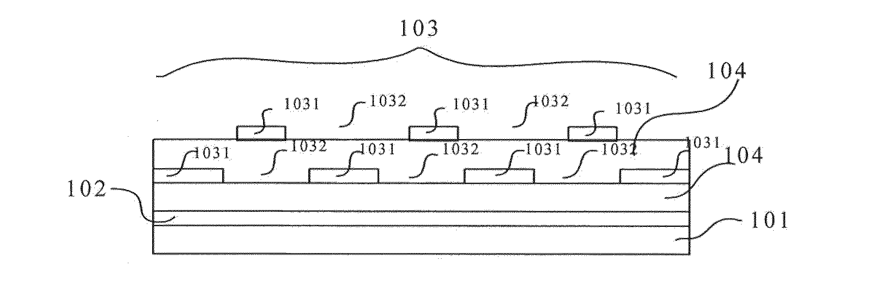
[0029]As shown in FIG. 3, the present embodiment provides a pixel structure comprising a slit electrode 103 and a plate electrode 102. The slit electrode 103 includes at least two layers, each of which includes a plurality of strip-shaped electrode sections 1031 and a plurality of slits 1032 sandwiched between adjacent electrode sections 1031, the electrode sections 1031 in an upper layer is positioned over the slits 1032 in a lower layer, and none of projections on. the substrate 101, of the electrode sections 1031 in the layers, are overlapped with each other. The plate electrode 102 is provided under the slit electrode 103 and separated from the slit electrode 103 by an insulation layer 104. Obviously, the layers of the slit electrode 103 are separated with each other by the insulation layer(s) 104. The insulation layer 104 for separating the layers of the slit electrode 103 corresponds to a first insulation layer. The insulation layer 104 for separating the plate electrode 102 f...

embodiment 2

[0042]The present embodiment provides an array substrate comprising the pixel structure as described in the embodiment 1.

[0043]Obviously, other well-known components such as thin film transistor, scanning lines and so on should be included in the array substrate, the specific descriptions of which will be omitted herein.

[0044]Since the array substrate of the present embodiment comprises the pixel structure as described in the embodiment 1, it may achieve high-quality display.

embodiment 3

[0045]The present embodiment provides a display device comprising the array substrate as described in the embodiment 2. The display device may be any product or component with display function such as mobile phone, tablet, television, monitor, notebook PC, digital photo frame, navigator, and so on.

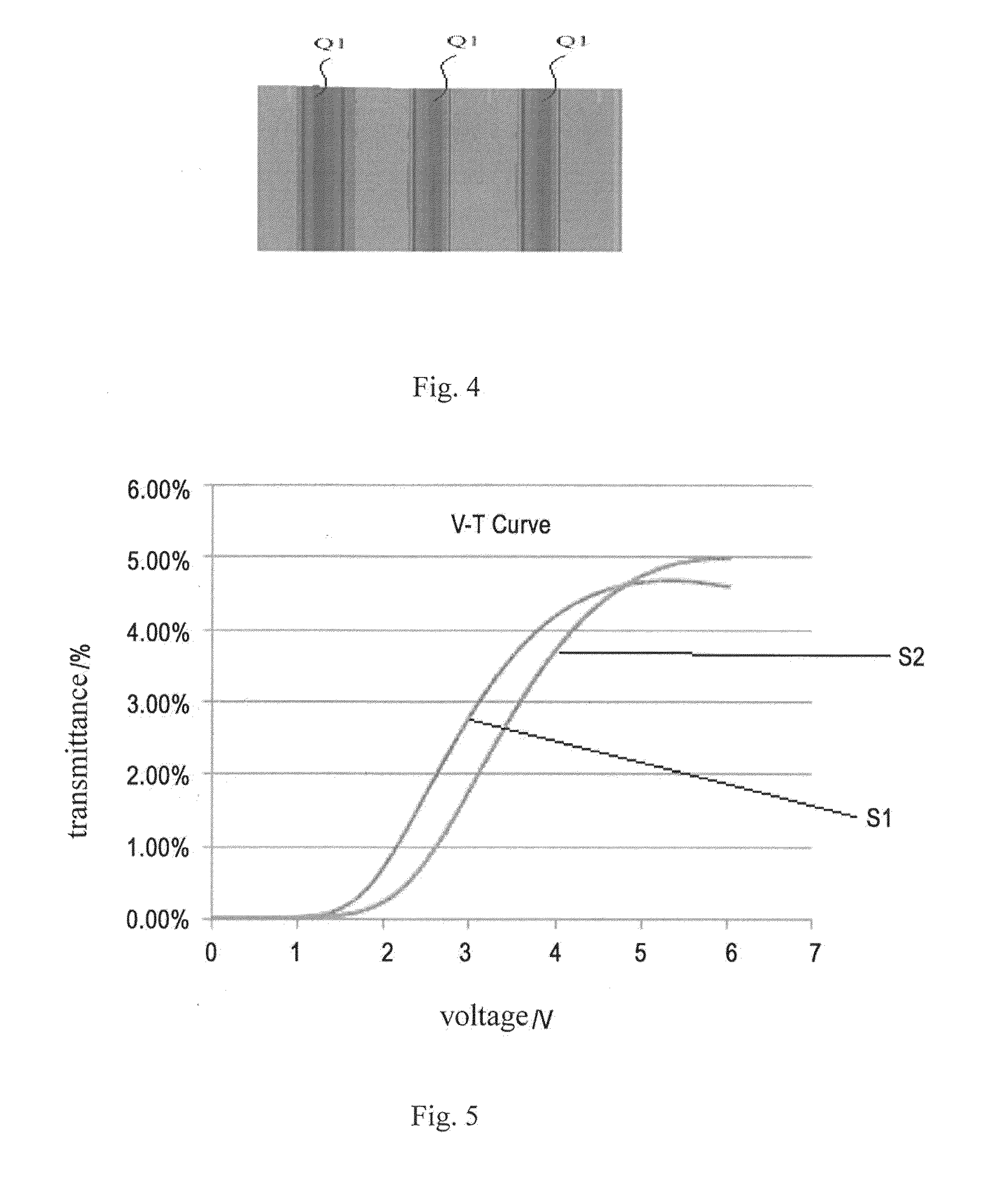
[0046]Since the display device of the embodiment comprises the array substrate of the embodiment 2, the area of the shadow zones Q1 is reduced, the transmittance is increased and the display effect of the screen is improved.

[0047]Obviously, the display device of the present embodiment may further include other conventional components such as power supply unit, display driver unit and so on.


PUM

PropertyMeasurementUnit
widthaaaaaaaaaa
widthaaaaaaaaaa
voltageaaaaaaaaaa

Abstract

A pixel structure, an array substrate and a display device are provided. The invention relates to the field of liquid crystal display technology, and can solve the problem of large shadow zones formed between slit electrodes in the existing pixel structure. The pixel structure of the invention comprises a slit electrode and a plate electrode. The slit electrode includes at least two layers, each of which includes a plurality of strip-shaped electrode sections and a plurality of slits located between the adjacent electrode sections, the electrode sections in an upper layer are positioned over the slits in a lower layer, projections of the electrode sections in the layers on a substrate are not overlapped with each other, and the layers are separated from each other by a first insulation layer. The plate electrode is provided under the slit electrode and separated from the slit electrode by a second insulation layer.

Description

FIELD OF THE INVENTION[0001]The present invention relates to the field of liquid crystal display technology, and particularly to a pixel structure, an array substrate and a display device.BACKGROUND OF THE INVENTION[0002]Thin Film Transistor Liquid Crystal Display (TFT-LCD) is a dominant Flat Panel Display (FPD).[0003]According to the direction of the electric field for driving liquid crystal, TFT-LCD may be classified into two categories: vertical electric field type and horizontal electric field type. As for the vertical electric field type TFT-LCD, it is required to form a pixel electrode on an array substrate and form a common electrode on a color substrate, while as for the horizontal electric field type TFT-LCD, it is required to form both the pixel electrode and the color substrate on the array substrate. The horizontal electric field type TFT-LCD, especially ADS type TFT-LCD is applied widely in the field of liquid crystal display technology due to its advantages such as wid...

Claims


Application Information

Patent Timeline
Patent Type & Authority Applications(United States)
IPC IPC(8): H01L27/12G02F1/1343G02F1/1362
CPCH01L27/124G02F1/136286G02F1/134309G02F1/134363
Inventor WANG, XUELU
Owner BOE TECH GRP CO LTD
Why Eureka
Try Eureka