Conductive film, display device equipped with same, and method for determining pattern of conductive film

a display device and conductive film technology, applied in the direction of conductive layers on insulating supports, identification means, instruments, etc., can solve the problems of inadequate improvement of moire visibility and the wiring pattern of conductive films, and achieve excellent visibility, suppress the occurrence of moire, and improve visibility

Inactive Publication Date: 2015-01-15
FUJIFILM CORP
View PDF2 Cites 26 Cited by
  • Summary
  • Abstract
  • Description
  • Claims
  • Application Information

AI Technical Summary

Benefits of technology

[0022]As described above, according to the present invention, it is possible to suppress the occurrence of moire to greatly improve visibility.
[0023]That is, in the present invention, since the frequency/intensities of moire is calculated from the peak frequencies/intensities obtained by frequency analysis of the pixel array pattern of the display device and the wiring pattern of the conductive film and the calculated intensity and frequencies of moire are numerically limited so as to obtain excellent visibility, it is

Problems solved by technology

Since human perception of moire is influenced by intensity as well as frequency, moire may be visually recognized depending on the intensity even at a frequency at which moire is not determined to be visually recognized in JP 2009-117683 A, and thus there is a problem in that the wiring pattern of the conductive film is not adequately improved in visibility of moire.
Particul

Method used


Image

  • Conductive film, display device equipped with same, and method for determining pattern of conductive film
  • Conductive film, display device equipped with same, and method for determining pattern of conductive film
  • Conductive film, display device equipped with same, and method for determining pattern of conductive film

Examples


first embodiment

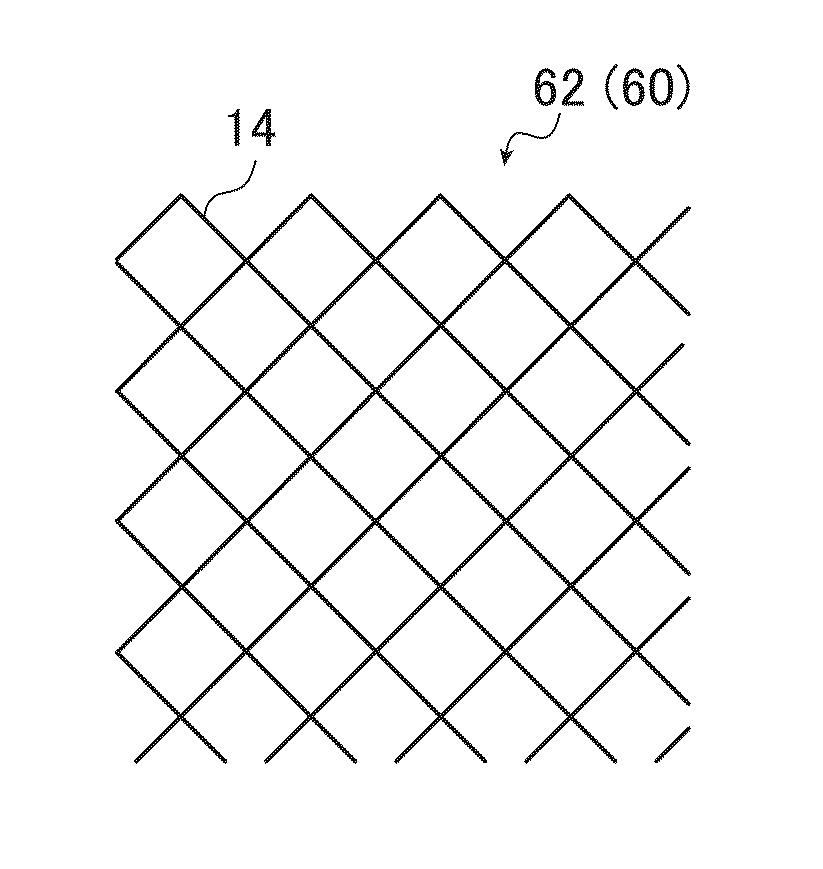
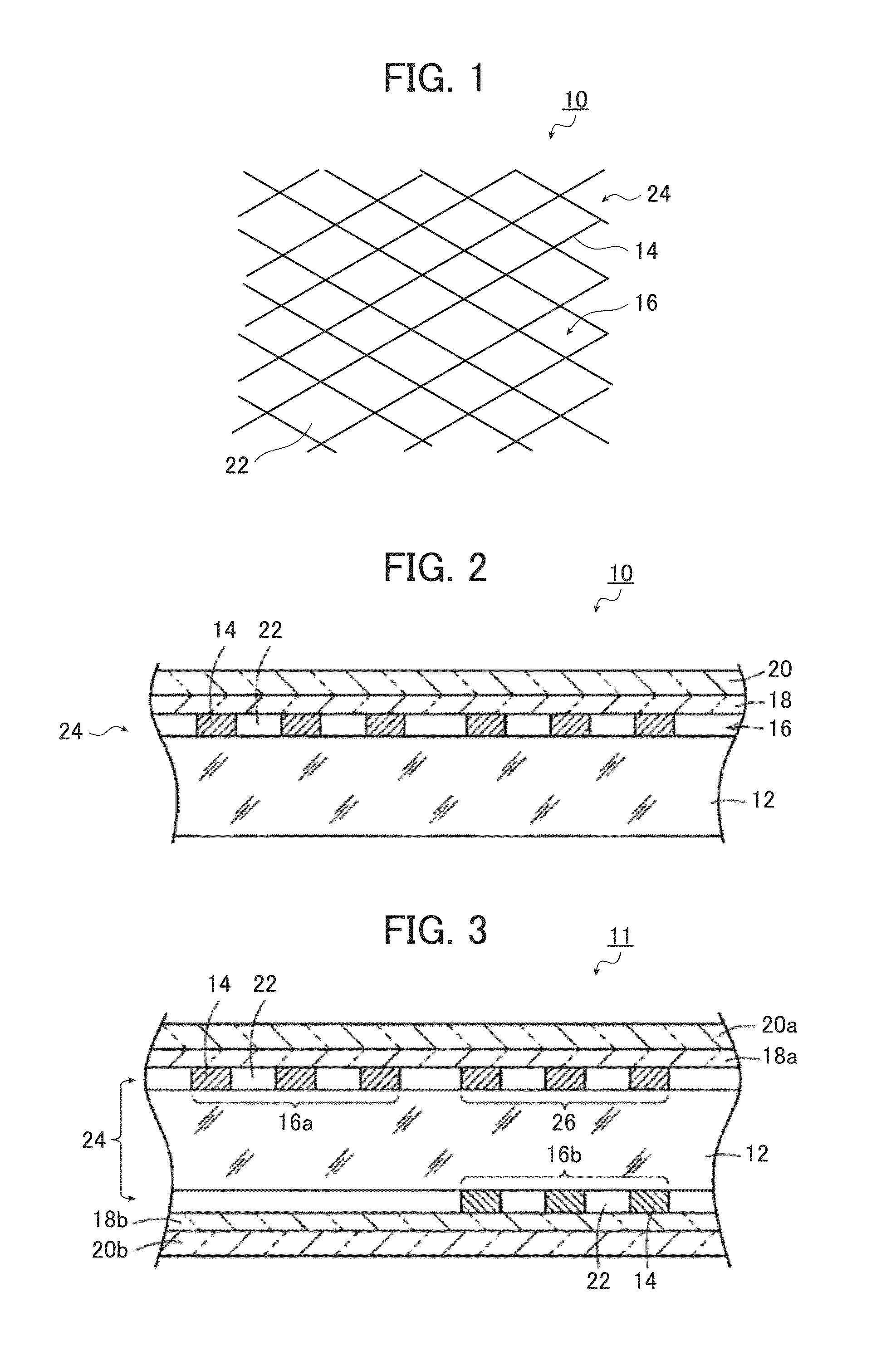
[0040]FIGS. 1 and 2 are respectively a plan view schematically illustrating an example of a conductive film according to the present invention and a schematic partial cross-sectional view thereof.

[0041]A conductive film 10 according to this embodiment illustrated in the drawings is to be installed on a display unit of a display device and is a conductive film having a wiring pattern that is excellent in suppression of occurrence of moire with respect to a black matrix (BM) of the display unit, particularly, a wiring pattern that is optimized in terms of visibility of moire with respect to the BM pattern when it is superimposed on the BM pattern. The conductive film 10 includes a transparent substrate 12, a conductive portion 16 that is formed on one surface of the transparent substrate 12 (surface on the upper side in FIG. 2) and that is composed of plural thin wires made of metal (hereinafter referred to as “thin metal wires”) 14, and a protective layer 20 bonded to the substantial...

second embodiment

[0051]As illustrated in the drawing, a conductive film 11 includes a first conductive portion 16a and a dummy electrode portion 26 formed on one surface (on the upper side in FIG. 3) of a transparent substrate 12, a second conductive portion 16b formed on the other surface (on the lower side in FIG. 3) of the transparent substrate 12, a first protective layer 20a bonded to the substantially entire surface of the first conductive portion 16a and the dummy electrode portion 26 through a first adhesive layer 18a, and a second protective layer 20b boned to the substantially entire surface of the second conductive portion 16b through a second adhesive layer 18b.

[0052]In the conductive film 11, the first conductive portion 16a and the dummy electrode portion 26 are each composed of plural thin metal wires 14 and formed on one surface (on the upper side in FIG. 3) of the transparent substrate 12, and the second conductive portion 16b is composed of plural thin metal wires 14 and formed o...


PUM


Abstract

The conductive film has a wiring pattern which, with respect to the frequencies and intensities of moire obtained by applying a human visual response characteristic to the frequency information and intensity information of moire calculated from peak frequencies and peak intensities of the two-dimensional Fourier spectrums of the transmittance image data of the wiring pattern and the transmittance image data of a pixel array pattern, causes the sum of intensities of moire each corresponding to frequencies of moire falling within a frequency range predetermined depending on the visual response characteristic to be less than or equal to a predetermined value. The conductive film allows suppression of moire and significant improvement in visibility.

Description

CROSS-REFERENCE TO RELATED APPLICATIONS[0001]This application is a continuation of International Application No. PCT / JP2013 / 055036 filed on Feb. 27, 2013, which claims priority under 35 U.S.C. §119(a) to Japanese Patent Application No. 2012-082711 filed on Mar. 30, 2012. Each of the above applications is hereby expressly incorporated by reference, in its entirety, into the present application.BACKGROUND OF THE INVENTION[0002]The present invention relates to a conductive film, a display device equipped with the conductive film, and a method for determining a pattern of the conductive film.[0003]Examples of a conductive film installed on a display unit of a display device (hereinafter also referred to as “display”) include a conductive film for electromagnetic shields and a conductive film for touch panels (for example, see JP 2009-117683 A and JP 2011-216379 A).[0004]JP 2009-117683 A, a published patent application filed by the same applicant as the present application, discloses tha...

Claims


Application Information

Patent Timeline
IPC IPC(8): G02B27/60G06F17/50G02B27/00
CPCG02B27/60G02B27/0012G06F17/5081G06F2217/06H05K9/0096G06F2203/04112G02B27/00G06F2203/04107G02B2207/121G06F3/0443G06F3/0445G06F3/0412G06F3/044G09F9/00H01B5/14G06F30/398G06F2111/04
Inventor IWAMI, KAZUCHIKASATO, RYOHEI
Owner FUJIFILM CORP
Why Eureka
Try Eureka