Wiring board

a technology of wire board and wire, applied in the direction of resist details, printed circuit aspects, non-metallic protective coating applications, etc., can solve the problem of short circuit between these connection terminals, and achieve the effect of reducing the pitch

Active Publication Date: 2015-01-29
NGK SPARK PLUG CO LTD
View PDF4 Cites 7 Cited by
  • Summary
  • Abstract
  • Description
  • Claims
  • Application Information

AI Technical Summary

Benefits of technology

[0017]As described above, according to the present invention, there can be provided a wiring substrate which can prev...

Problems solved by technology

However, when a plurality of connection terminals are arranged in a single opening at small pitches, solder applied (through coating) onto the f...

Method used


Image

  • Wiring board
  • Wiring board
  • Wiring board

Examples


first embodiment

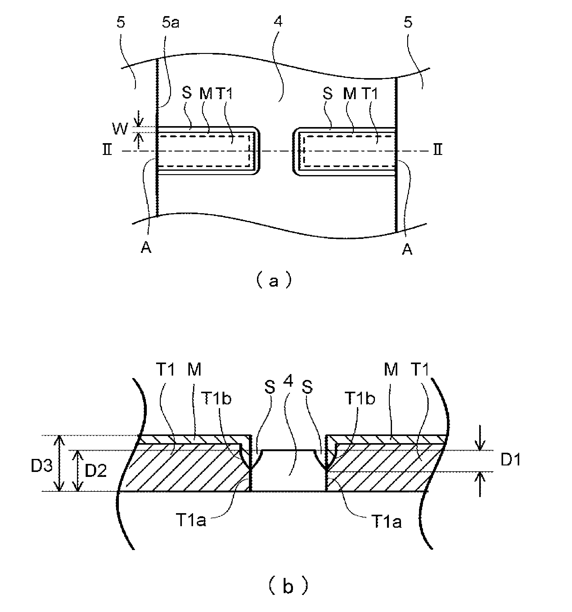
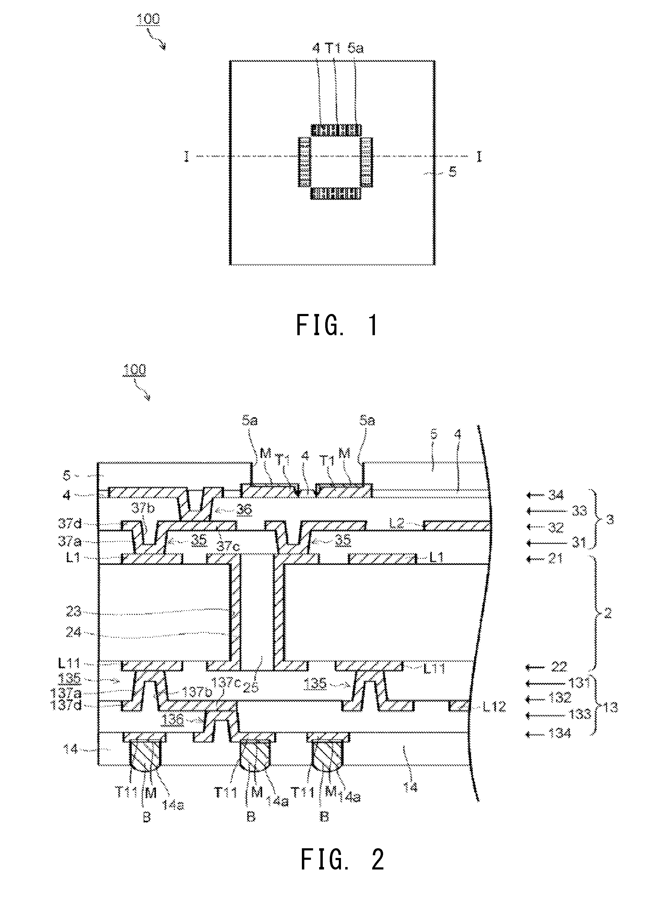
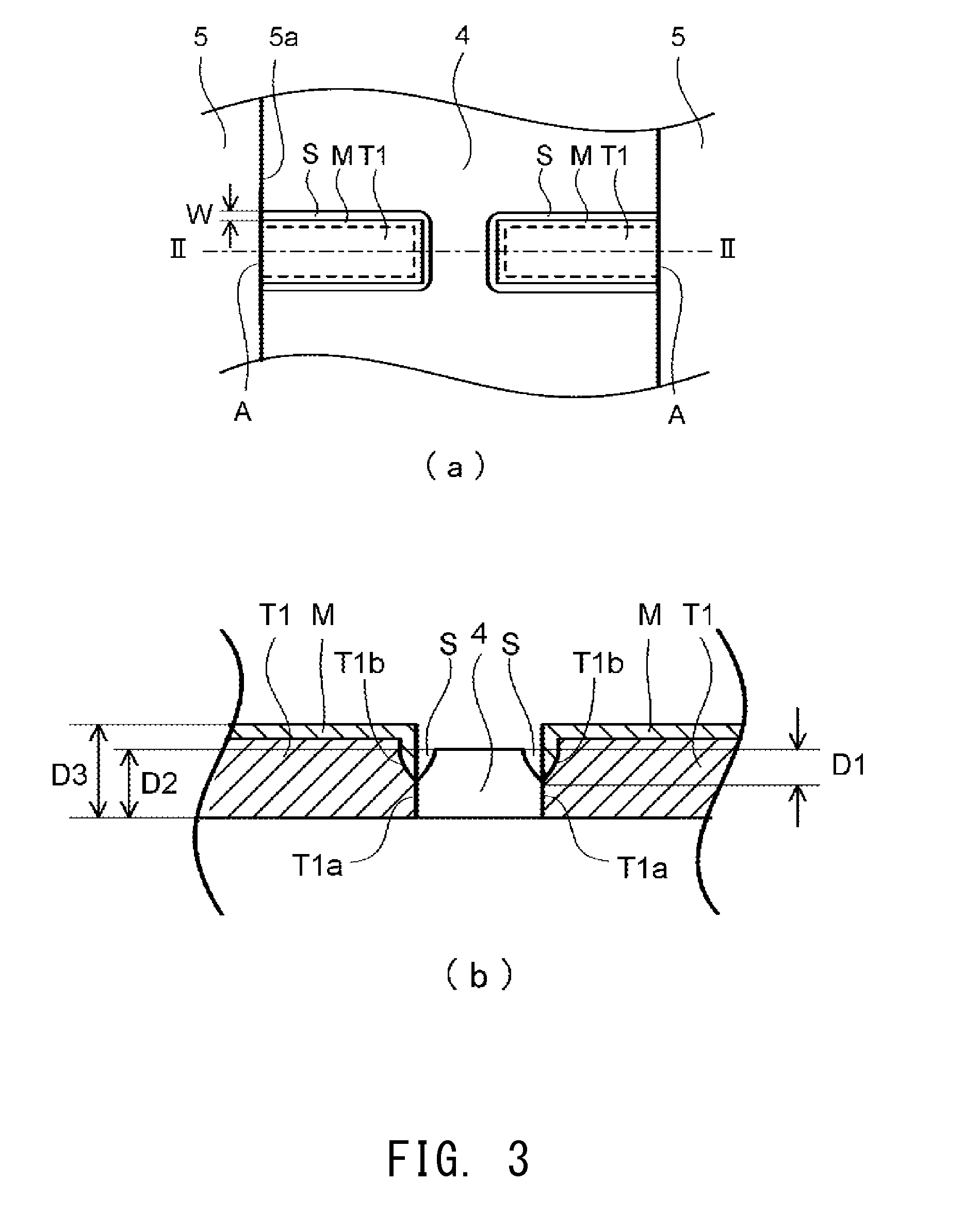
[0042]FIG. 1 is a plan view (on the front surface side) of a wiring substrate 100 according to the first embodiment. FIG. 2 is a partially cross-sectional view of the wiring substrate 100 taken along line I-I of FIG. 1. FIG. 3 shows the configuration of connection terminals T1 formed on the front surface side of the wiring substrate 100. FIG. 3(a) is a top view of the connection terminals T1. FIG. 3(b) is a cross-sectional view taken along line II-II of FIG. 3(a). In the following description, the side on which semiconductor chips are connected is referred to as the front surface side, and the side on which a motherboard, a socket, or the like (hereinafter referred to as a “motherboard or the like”) is connected is referred to as the back surface side.

[0043](Configuration of wiring substrate 100) The wiring substrate 100 shown in FIGS. 1 to 3 includes a core substrate 2; a build-up layer 3 (on the front surface side) on which are formed a plurality of connection terminals T1 for con...

second embodiment

[0096]FIG. 15 is a plan view (on the front surface side) of a wiring substrate 200 according to the second embodiment. FIG. 16 is a partially cross-sectional view of the wiring substrate 200 taken along line I-I of FIG. 15. FIG. 17 shows the configuration of connection terminals T2 formed on the front surface side of the wiring substrate 200. FIG. 17(a) is a top view of the connection terminals T2. FIG. 17(b) is a cross-sectional view taken along line II-II of FIG. 17(a). Although the configuration of the wiring substrate 200 will next be described with reference to FIGS. 15 to 17, the same components as employed in the wiring substrate 100 (which has been described with reference to FIGS. 1 to 3) are denoted by the same reference numerals, and repeated description thereof is omitted.

[0097](Configuration on front surface side) On the front surface side of the wiring substrate 200, a cover plating layer 41 electrically connected to a core conductor layer 21 is formed, and the cover p...

third embodiment

[0106]FIG. 18 is a plan view (on the front surface side) of a wiring substrate 300 according to the third embodiment. FIG. 19 is a partially cross-sectional view of the wiring substrate 300 taken along line I-I of FIG. 18. FIG. 20 shows the configuration of connection terminals T3 formed on the front surface side of the wiring substrate 300. FIG. 20(a) is a top view of the connection terminals T3. FIG. 20(b) is a cross-sectional view taken along line II-II of FIG. 20(a).

[0107]The wiring substrate 300 according to the third embodiment differs from the wiring substrate 200 described above with reference to FIGS. 15 to 17 in that connection terminals T3 and T11 are formed directly on conductor layers 32 and 132, respectively, without the intervention of vias. Although the configuration of the wiring substrate 300 will next be described with reference to FIGS. 18 to 20, components common between the wiring substrate 300 and the wiring substrate 100 (which has been described with referen...


PUM


Abstract

To provide a wiring substrate which can prevent short circuit between connection terminals, and which realizes reduction of the pitch between the connection terminals. The wiring substrate of the present invention includes a layered structure including one or more insulation layers and one or more conductor layers, and the wiring substrate is characterized in that a plurality of connection terminals are formed on the layered structure so as to be separated from one another; a filling member is filled between the connection terminals; and each of the connection terminals has a side surface composed of a contact surface which is in contact with the filling member, and a spaced surface which is not in contact with the filling member and which is located above the contact surface and below the top surface of the filling member.

Description

TECHNICAL FIELD[0001]The present invention relates to a wiring substrate having, on a main surface thereof, a plurality of terminals for connection to semiconductor chips.BACKGROUND ART[0002]Generally, a wiring substrate has, on a main surface (front surface) thereof, terminals for connection to semiconductor chips (hereinafter may be referred to as “connection terminals”). In recent years, connection terminals have been provided at high packing density, and the distance (pitch) between adjacent connection terminals has been reduced. Thus, there has been proposed a wiring substrate having an NSMD (non-solder mask defined) structure in which a plurality of connection terminals are arranged in a single opening of a solder resist layer.[0003]However, when a plurality of connection terminals are arranged in a single opening at small pitches, solder applied (through coating) onto the front surface of a connection terminal may flow toward an adjacent connection terminal, and short circuit...

Claims


Application Information

Patent Timeline
IPC IPC(8): H05K1/02
CPCH05K1/0213H05K3/28H01L23/49822H01L23/49827H01L2924/0002H05K3/244H05K3/3452H05K2201/09881H05K2201/099H05K2203/0571H05K2203/0588H01L23/49816H05K1/111H01L23/49811H01L2924/00012H01L2924/00H01L23/12H05K3/34
Inventor NISHIDA, TOMOHIROMORI, SEIJIWAKAZONO, MAKOTO
Owner NGK SPARK PLUG CO LTD
Why Eureka
Try Eureka