Liquid crystal display device and method for producing the same
a display device and liquid crystal technology, applied in the manufacture of electrode systems, electric discharge tubes/lamps, instruments, etc., can solve the problems of display failure, overall response speed is insufficient, and transmittance degradation, etc., to suppress ghosting, high response speed, and less drop marks
- Summary
- Abstract
- Description
- Claims
- Application Information
AI Technical Summary
Benefits of technology
Problems solved by technology
Method used
Image
Examples
example 1
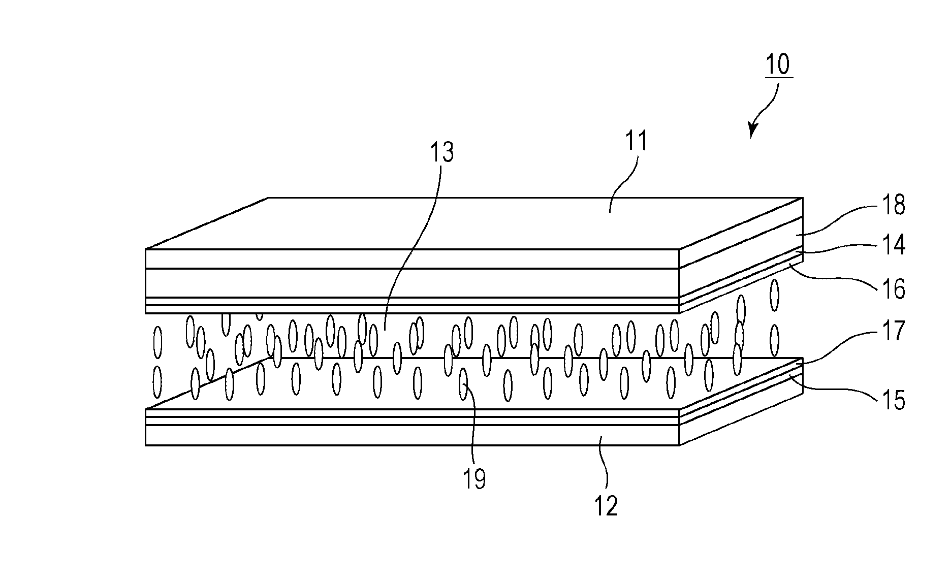
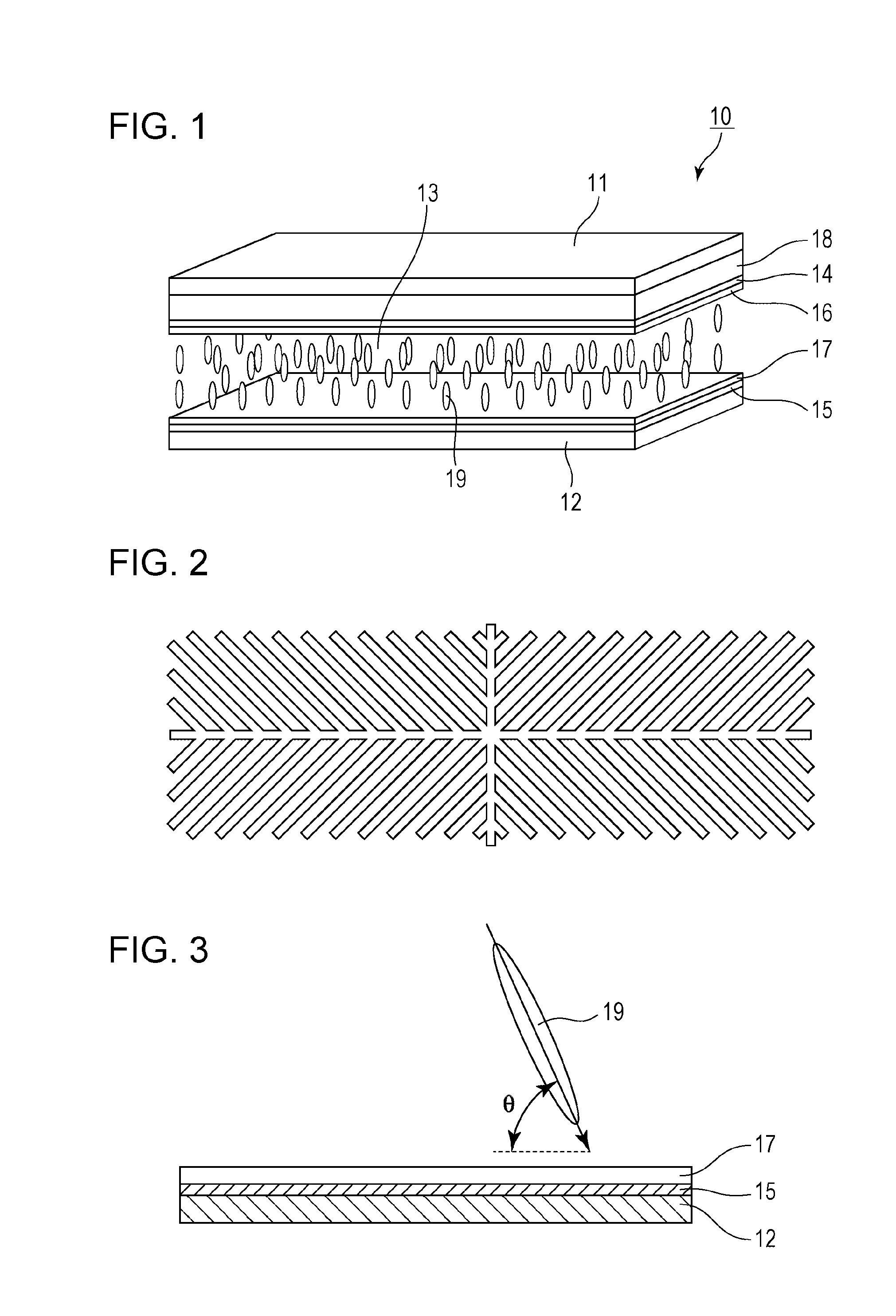
[0167]A first substrate (common electrode substrate) that has a transparent electrode layer constituted by a transparent common electrode and a color filter layer and a second substrate (pixel electrode substrate) having a pixel electrode layer that includes transparent pixel electrodes driven by active elements were made.
[0168]Each pixel electrode of the pixel electrode substrate was made by etching ITO so that slits having no electrodes were formed in the pixel electrode to align liquid crystal molecules in different directions.
[0169]A vertical alignment film material that contains a polyimide precursor and a polymerizable compound having a reactive group was applied to each of the common electrode substrate and the pixel electrode substrate by a spin coating method. The applied films were heated at 200° C. to cure the polyimide precursor in the vertical alignment film material and form a 100 nm vertical alignment film on a surface of each substrate. At this stage, the polymerizab...
example 2
[0195]A liquid crystal display device of Example 2 was obtained as in Example 1 except that a polyimide solution (trade name: JALS2131-R6, produced by JSR) containing 3% of a polyimide precursor and a solution containing 3% of a polymerizable compound having a reactive group represented by formula (V-4a) below were used as the vertical alignment film forming material.
[0196]The liquid crystal display device of Example 2 was evaluated in terms of ghosting and drop marks as in Example 1. The results are shown in Table 8.
[0197]The results show that the liquid crystal display device of Example 2 was slightly inferior to the liquid crystal display device of Example 1 but exhibited high response speed, suppressed drop marks, and was resistant to ghosting.
TABLE 8Drop mark evaluationAGhosting evaluationAResponse speed / ms8.3
example 3
[0198]A liquid crystal display device of Example 3 was obtained as in Example 1 except that a polyimide solution (trade name: JALS2131-R6, produced by JSR) containing 3% of a polyimide precursor and a solution containing 3% of a polymerizable compound having a reactive group represented by formula (V-6a) below were used as the vertical alignment film forming material.
[0199]The liquid crystal display device of Example 3 was evaluated in terms of ghosting and drop marks as in Example 1. The results are shown in Table 9.
[0200]The results show that the liquid crystal display device of Example 3 was slightly inferior to the liquid crystal display device of Example 1 but exhibited high response speed, suppressed drop marks, and was resistant to ghosting.
TABLE 9Drop mark evaluationAGhosting evaluationAResponse speed / ms8.2
PUM
| Property | Measurement | Unit |
|---|---|---|
| mass % | aaaaa | aaaaa |
| mass % | aaaaa | aaaaa |
| mass % | aaaaa | aaaaa |
Abstract
Description
Claims
Application Information


