Stacked multi - chip packaging structure and manufacturing method thereof

a technology of packaging structure and multi-chip, applied in the direction of semiconductor/solid-state device testing/measurement, semiconductor device details, semiconductor/solid-state device testing/measurement, etc., can solve the problems of lower device electrical efficiency and higher electrical and thermal resistan

Active Publication Date: 2015-02-05
ALPHA & OMEGA SEMICON INC
View PDF3 Cites 30 Cited by
  • Summary
  • Abstract
  • Description
  • Claims
  • Application Information

AI Technical Summary

Problems solved by technology

However, in a DC-DC converter, a high-side MOSFET chip and a low-side MOSFET chip and an IC controller chip are arranged side by side on the same plane surface of a lead frame and are co-packaged inside a plastic package body, which requires a larger package size and results in higher electrical and thermal resistance due to wire bonding, thus the device electrical efficiency is lower.

Method used


Image

  • Stacked multi - chip packaging structure and manufacturing method thereof
  • Stacked multi - chip packaging structure and manufacturing method thereof
  • Stacked multi - chip packaging structure and manufacturing method thereof

Examples


embodiment 1

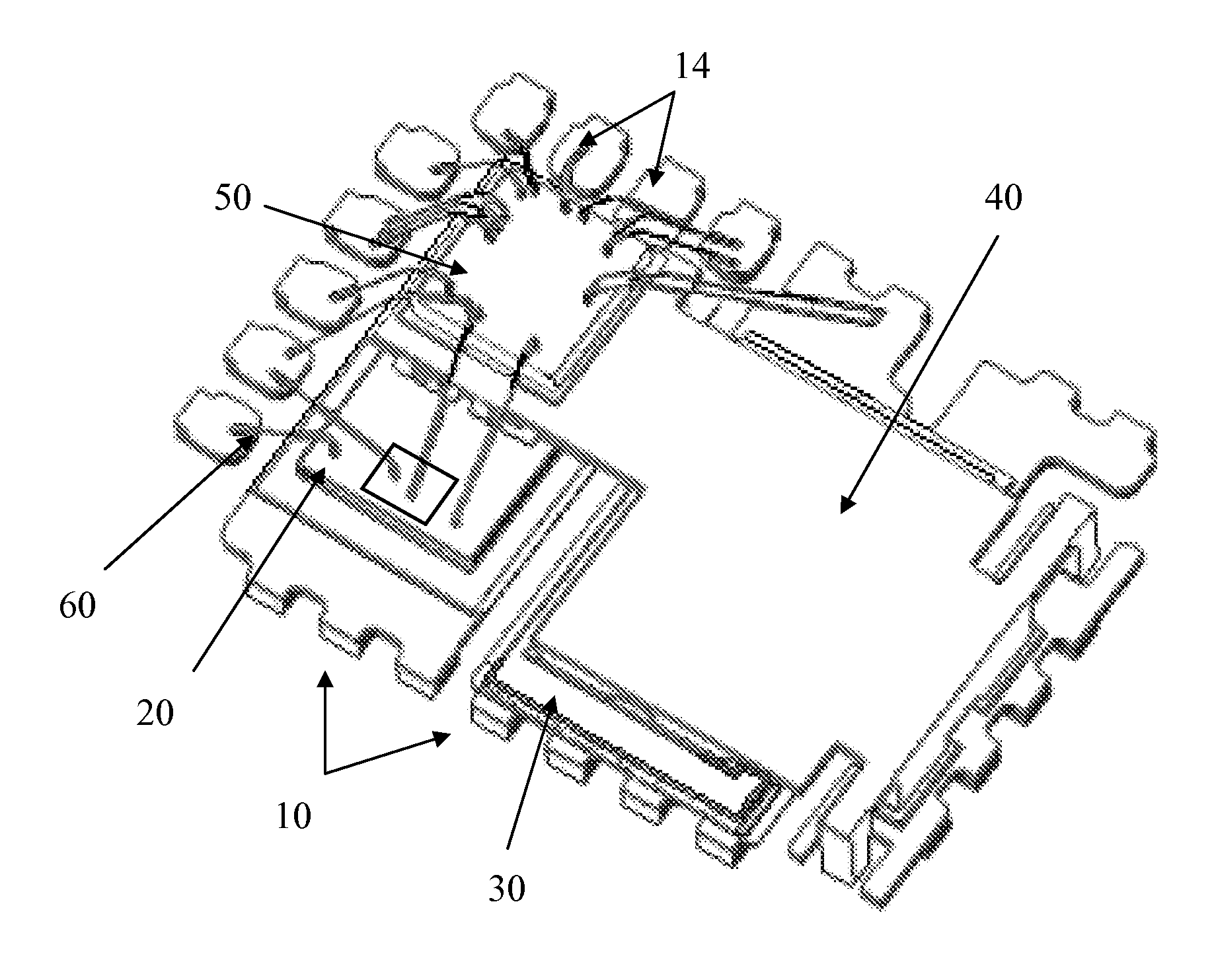
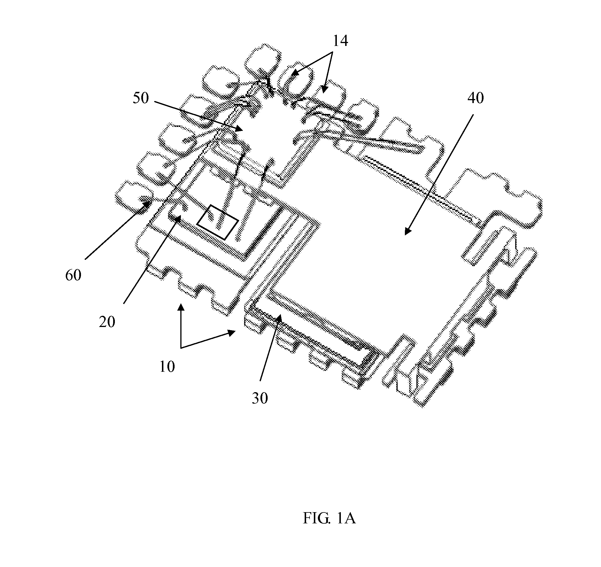
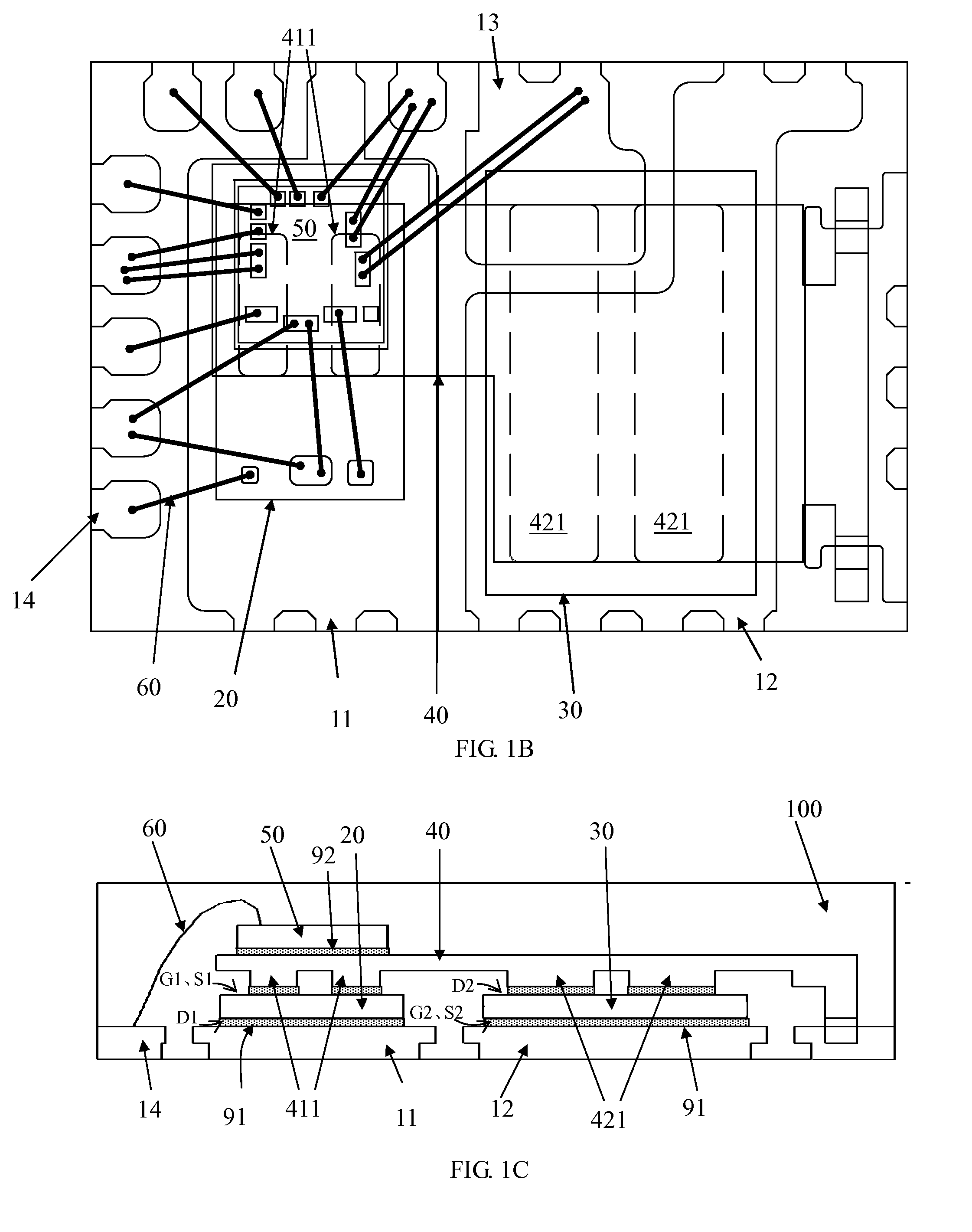
[0018]As shown in FIG. 1A-FIG. 1C, according to the present invention, HS MOSFET 20 and LS MOSFET 30 of same type (N-type or P-type) are attached on two separate paddles 11 and 12 of a lead frame 10. An IC controller 50 is stacked on the two MOSFETs 20 and 30 through a metal clip 40, and is electrically connected with the corresponding electrodes of the LS MOSFET 30 and the HS MOSFET 20 and a pin 14 of the lead frame 10 through bonding wires 60. The HS MOSFET 20, LS MOSFET 30, and the IC controller 50 are then packaged inside a plastic package body 100 forming a DC-DC converter.

[0019]Each of the HS chip 20 and LS chip 30 includes a source electrode and a gate electrode at the front surface and a drain electrode at the back surface. Both of the gate electrodes G1 and G2 of the HS chip 20 and LS chip 30 are connected to a control electrode on the IC chip 50, the drain electrode D1 of the HS chip 20 is connected to a Vin end, the source electrode 51 is connected to the drain electrode ...

embodiment 2

[0040]FIG. 4A-FIG. 4G are schematic diagrams showing the steps of a method for forming a stacked multi-chip package device according to an alternative embodiment and FIG. 5 is a flow diagram of the packaging method of FIGS. 4A-4G. FIG. 4A is a schematic diagram of a lead frame 10 that includes a first die paddle 11 and a second die paddle 12. As shown in FIG. 4B, the HS chip 20 is attached on the first die paddle 11, where the drain electrode D1 at the back surface is electrically connected to the first die paddle 11. The second die paddle includes the first part 12 and the second part 13, and a LS chip 30 is flipped and attached on the first part 12 and the second part 13 with the source electrode S2 and the gate electrode G2 at the front surface of the flipped LS chip 30 electrically connected with the first part 12 and the second part 13 of the second die paddle respectively as shown in FIG. 4C. As shown in FIG. 4D, a metal clip 40 is attached on the HS chip 20 and the LS chip 30...

embodiment 3

[0043]FIG. 6A-FIG. 6H are schematic diagrams showing the steps of a method for forming a stacked multi-chip package device according to an alternative embodiment and FIG. 7 is a flow diagram of the packaging method of FIG. 6A-FIG. 6H. As shown in FIG. 6A, the lead frame 10 includes the first die paddle 11 and a second die paddle that includes a first part 12 and a second part 13. As shown in FIG. 6B, a HS chip 20 is attached with the drain D1 at the back surface being electrically connected on the first die paddle 11. As shown in FIG. 6C, a LS chip 30 is flipped and attached with the source S2 and the gate G2 at the front surface being electrically connected on the second die paddle. As shown in FIG. 6D, a metal clip 40, including a high-side connecting part 41, a low-side connecting part 42 and a pin connecting part 43, is mounted on the HS chip 20 and the LS chip 30, so that the high-side connecting part 41 is electrically connected with the source S1 at the front surface of the H...


PUM


Abstract

A stacked multi-chip packaging structure comprises a lead frame, a first semiconductor chip mounted on the lead frame, a second semiconductor chip flipped-chip mounted on the lead frame, a metal clip mounted on top of the first and second semiconductor chips and a third semiconductor chip stacked on the meal clip; bonding wires electrically connecting electrodes on the third semiconductor chip to the first and second semiconductor chips and the pins of the lead frame; plastic molding encapsulating the lead frame, the chips and the metal clip.

Description

FIELD OF THE INVENTION[0001]The present invention relates to the semiconductor device, and in particular, to a stacked multi-layer packaging structure and a manufacturing method thereof.DESCRIPTION OF THE RELATED ART[0002]Generally, a DC-DC converter includes two MOSFETs (Metal-Oxide-Semiconductor Field Effect Transistor), one of which is a high-side MOSFET (hereinafter referred to as HS MOSFET) and the other is a low-side MOSFET (hereinafter referred to as LS MOSFET). The gate electrode G1 of the HS MOSFET and the gate electrode G2 of the LS MOSFET are connected with an IC controller and the drain electrode D1 of the HS MOSFET is connected with a Vin end, the source electrode 51 is connected with the drain electrode D2 of the LS MOSFET, while the source electrode S2 of the LS MOSFET is connected with a Gnd end.[0003]However, in a DC-DC converter, a high-side MOSFET chip and a low-side MOSFET chip and an IC controller chip are arranged side by side on the same plane surface of a lea...

Claims


Application Information

Patent Timeline
Patent Type & Authority Applications(United States)
IPC IPC(8): H01L23/495H01L23/00
CPCH01L24/81H01L23/49534H01L2224/32245H01L2224/48145H01L2224/48247H01L2224/73265H01L24/49H01L2224/40137H01L2224/37013H01L24/05H01L24/06H01L24/33H01L24/37H01L24/40H01L24/48H01L24/97H01L2224/05553H01L2224/05554H01L2224/0603H01L2224/48091H01L2224/48465H01L2224/49111H01L2224/49113H01L2224/73263H01L2924/00014H01L2924/07802H01L2924/0781H01L2924/13055H01L2924/13091H01L2224/40247H01L2224/40145H01L23/4334H01L23/492H01L23/49524H01L23/49562H01L23/49575H01L2924/1305H01L2224/85H01L2224/40095H01L2224/37147H01L2924/181H01L2224/40245H01L2224/0401H01L2224/04042H01L24/73H01L2224/97H01L2224/83801H01L2224/84801H01L24/41H01L25/50H01L2224/8385H01L24/84H01L2924/18301H01L2224/84345H01L2224/73221H01L2924/00012H01L2924/00H01L2224/45099H01L25/07H01L21/304H01L21/56H01L21/78H01L22/14H01L23/3675H01L23/49503H01L24/11H01L24/27H01L24/83H01L24/85H01L25/0652H01L2224/118H01L2224/13022H01L2224/48106H01L2224/48177H01L2224/49171H01L2224/83851H01L2225/06506H01L2225/0651H01L2225/06572H01L2225/06589
Inventor ZHANG, XIAOTIANPAN, HUALU, MING-CHENLU, JUNYILMAZ, HAMZA
Owner ALPHA & OMEGA SEMICON INC
Why Eureka
Try Eureka