Long-term packaging for the protection of implant electronics

a technology for protecting electronics and implants, applied in the direction of eye treatment, electrical apparatus casings/cabinets/drawers, semiconductor/solid-state device details, etc., can solve the problems of loss of elastic flexibility and thickening of parylene-c coated bio-compatible silicone layers, and achieve the effect of reducing the water vapor transmission rate (wvtr)

Active Publication Date: 2015-02-05
CALIFORNIA INST OF TECH
View PDF8 Cites 18 Cited by
  • Summary
  • Abstract
  • Description
  • Claims
  • Application Information

AI Technical Summary

Benefits of technology

[0019]In one embodiment, the present invention provides a protective architecture such as a corrosion barrier in conjunction with an encapsulation layer. In certain aspects, the corrosion barrier decreases the water vapor transmission rate (WVTR) even further than the encapsulation layer alone. The WVTR is one parameter that can aid in quantifying the effectiveness of an encapsulation layer(s) and / or a corrosion protection barrier.
[0020]In certain aspects, the present invention provides an encapsulating material layer together with a corrosion barrier to protect a micropackaged device or an implant from corrosive bodily fluid. The corrosion barrier can be a low-permeation material such as glass, metal such as a thin metal film, ceramic, parylene, silicone, PET, PVC or a combination thereof, which affords the implant even further protection over the encapsulation layer alone.

Problems solved by technology

However, the parylene-C coated bio-compatible silicone layer tends to be thick and can lose its elastic flexibility.

Method used


Image

  • Long-term packaging for the protection of implant electronics
  • Long-term packaging for the protection of implant electronics
  • Long-term packaging for the protection of implant electronics

Examples


Embodiment Construction

I. Embodiments

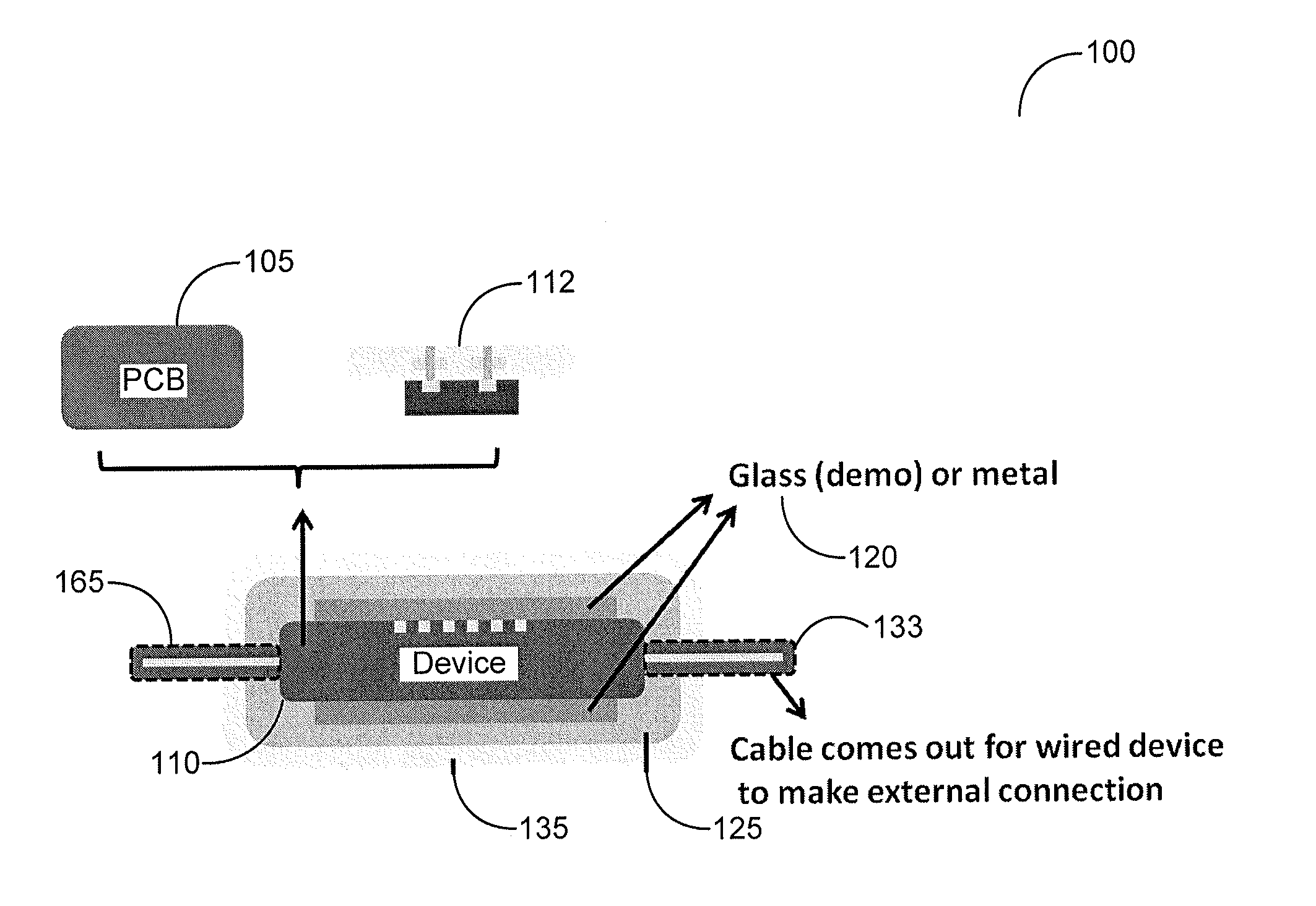
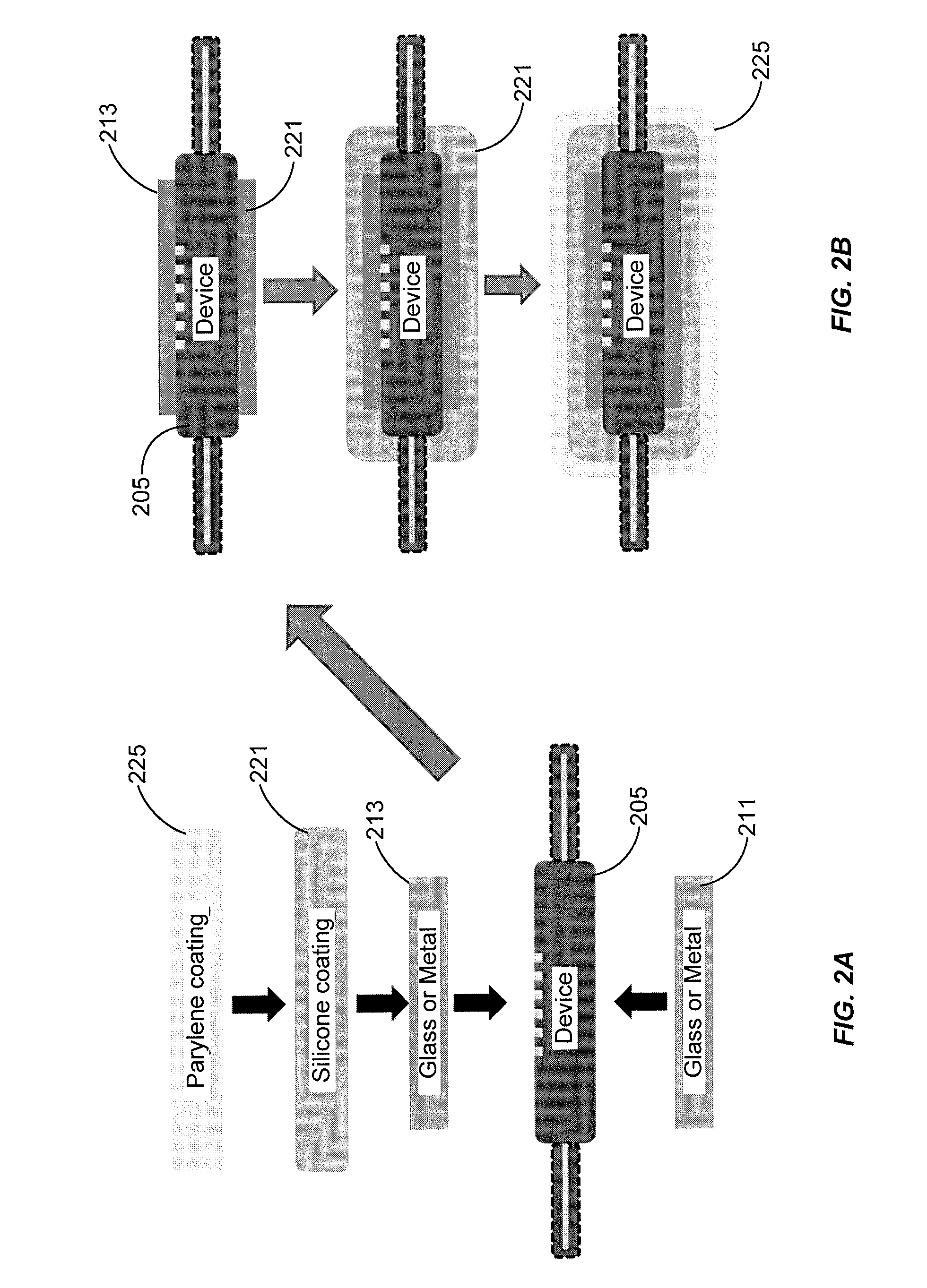
[0035]Aspects of the present invention are directed to a micropackaged electronic device(s) and / or component(s) for use as an implantable medical device. In some aspects, the electronics are hermetically sealed within a biocompatible housing. FIG. 1 illustrates one embodiment of the micropackaged device 100 of the present invention. In certain aspects, the micropackaged device 100 comprises a substrate for securing a device 110. A wide variety of devices can be packaged according to the present invention. Suitable devices include, but are not limited to, an integrated circuit (IC) chip, a printed circuit board (PCB), a microelectromechanical system (MEMS), a capacitor, an inductor, an oscillator, or a combination thereof. The devices to be protected can be a wired or a wireless PCB, thin-film integrated device, and the like. If the component or device is wireless (e.g., with a coil), the entire device can be totally encapsulated in the enclosure. Small electronic compo...


PUM

PropertyMeasurementUnit
resistanceaaaaaaaaaa
sizeaaaaaaaaaa
sizeaaaaaaaaaa

Abstract

The present invention provides a micropackaged device comprising: a substrate for securing a device; a corrosion barrier affixed to said substrate; optionally at least one feedthrough disposed in said substrate to permit at least one input and or at least one output line into said micropackaged device; and an encapsulation material layer configured to encapsulate the micropackaged device.

Description

CROSS-REFERENCES TO RELATED APPLICATIONS[0001]This application claims priority to U.S. Patent Application No. 61 / 862,180, filed Aug. 5, 2013, which is incorporated herein by reference for all purposes.STATEMENT AS TO RIGHTS TO INVENTIONS MADE UNDER FEDERALLY SPONSORED RESEARCH AND DEVELOPMENT[0002]This invention was made with government support under EEC-0310723 awarded by the National Science Foundation. The government has certain rights in the invention.BACKGROUND OF THE INVENTION[0003]Biocompatible silicones have been used as encapsulation layers for decades but it is known that most silicones tend to have a rather large water vapor transmission rate (WVTR) due to their porous structure. One way to reduce the WVTR by adding another parylene-C coating on silicone is reported to seal the silicone layer and have very good adhesion to it (see, S. Sawano et al., Digest Tech. Papers MEMS'08 Conference, Tucson, USA, Jan. 13-17, 2008, pp. 419-422). However, the parylene-C coated bio-comp...

Claims


Application Information

Patent Timeline
Patent Type & Authority Applications(United States)
IPC IPC(8): H05K5/06H05K3/40H05K1/11
CPCH05K5/065H05K3/4038H05K1/11A61F9/0017H05K1/032H05K3/0041H05K3/281H05K3/282H05K3/284H05K3/285H05K3/381H05K2201/017H05K2201/10015H05K2201/10022H05K2201/1003H05K2201/10075H05K2201/10083H05K2201/10287H05K2201/10356H05K2203/0139H05K2203/0514H05K2203/1316H05K2203/1322H05K2203/1338H01L2224/73204H01L2924/0002H01L23/3135Y10T29/49165H01L2924/00
Inventor TAI, YU-CHONGCHANG, HAN-CHIEH
Owner CALIFORNIA INST OF TECH
Why Eureka
Try Eureka