Semiconductor device

a technology of semiconductors and devices, applied in the direction of semiconductor devices, basic electric elements, electrical appliances, etc., can solve problems such as deterioration of on-resistance properties, and achieve the effect of wide process margins

Active Publication Date: 2015-02-12
TOYOTA JIDOSHA KK
View PDF0 Cites 9 Cited by
  • Summary
  • Abstract
  • Description
  • Claims
  • Application Information

AI Technical Summary

Benefits of technology

[0005]When the low concentration p-layer is provided along the end portions of the trench in the longitudinal direction of the trench, as disclosed in the Patent Document 1, and when the low concentration p-layer is in contact with the end portions of the trench in the longitudinal direction of the trench, the low concentration p-layer may be damaged and reduced in a step of manufacturing the semiconductor device, such as when a gate insulating film is formed. Therefore, it is necessary to secure a wide process margin. Further, when the low concentration p-layer is examined by an electron microscope or by SIMS during an inspection process, and when the low concentration p-layer is in contact with the end portions of the trench along the longitudinal direction of the trench, it is difficult to examine the low concentration p-layer due to an edge effect of the trench.

Problems solved by technology

A MOSFET having a floating structure at a bottom of a trench has the high voltage, but at the same time, it has a problem of deterioration in on-resistance property.

Method used


Image

  • Semiconductor device
  • Semiconductor device
  • Semiconductor device

Examples


first embodiment

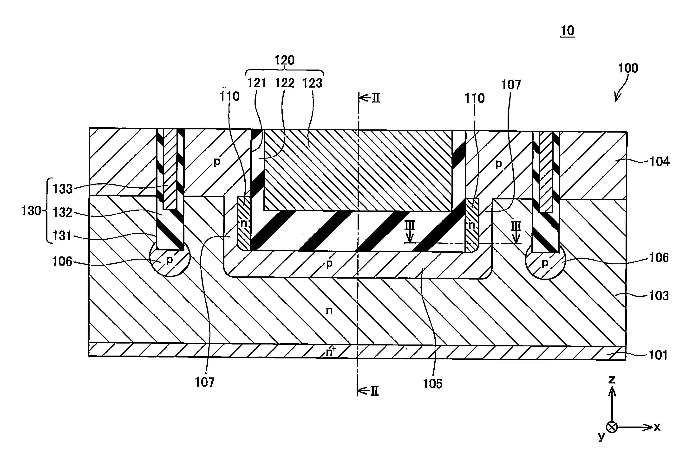
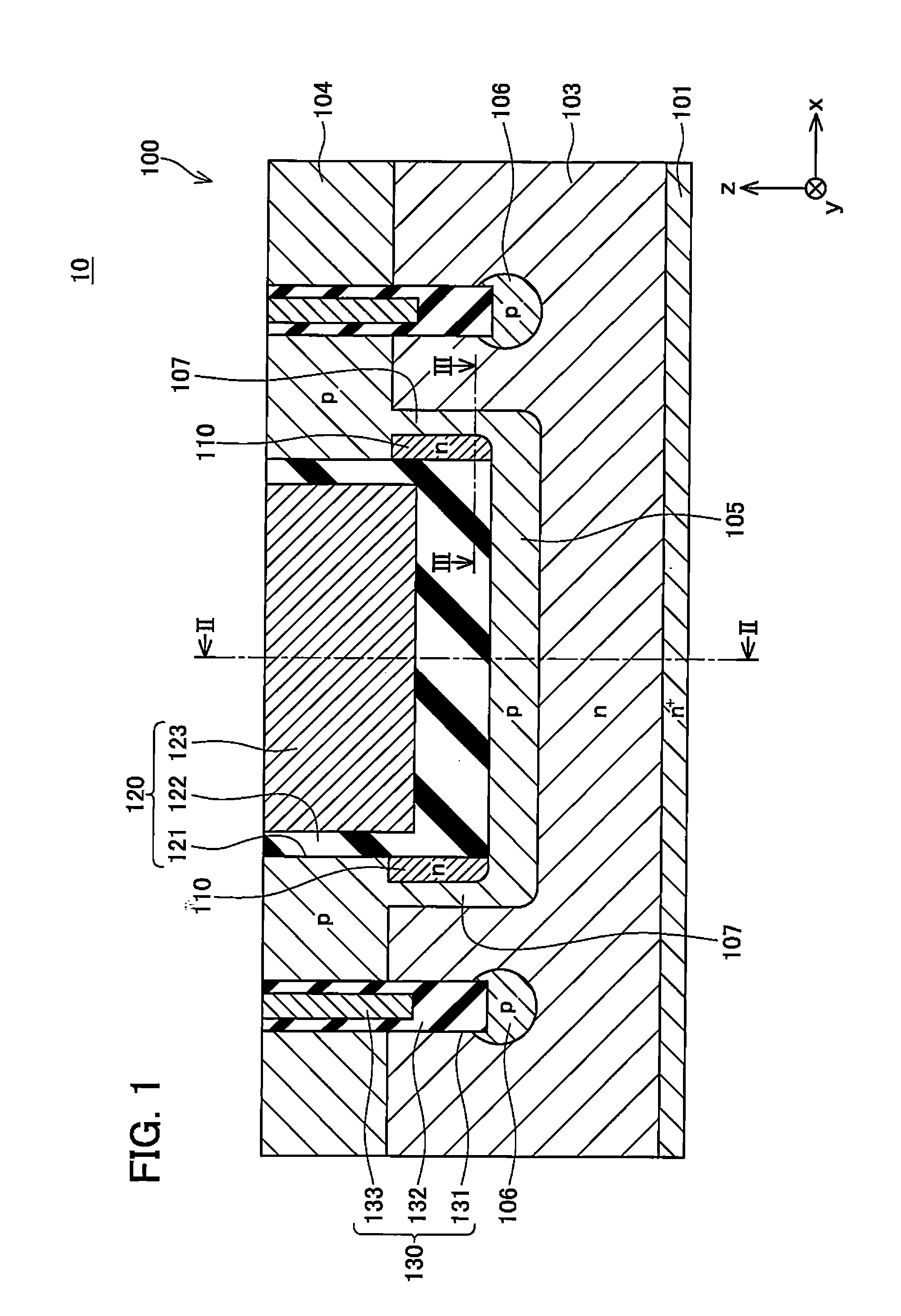
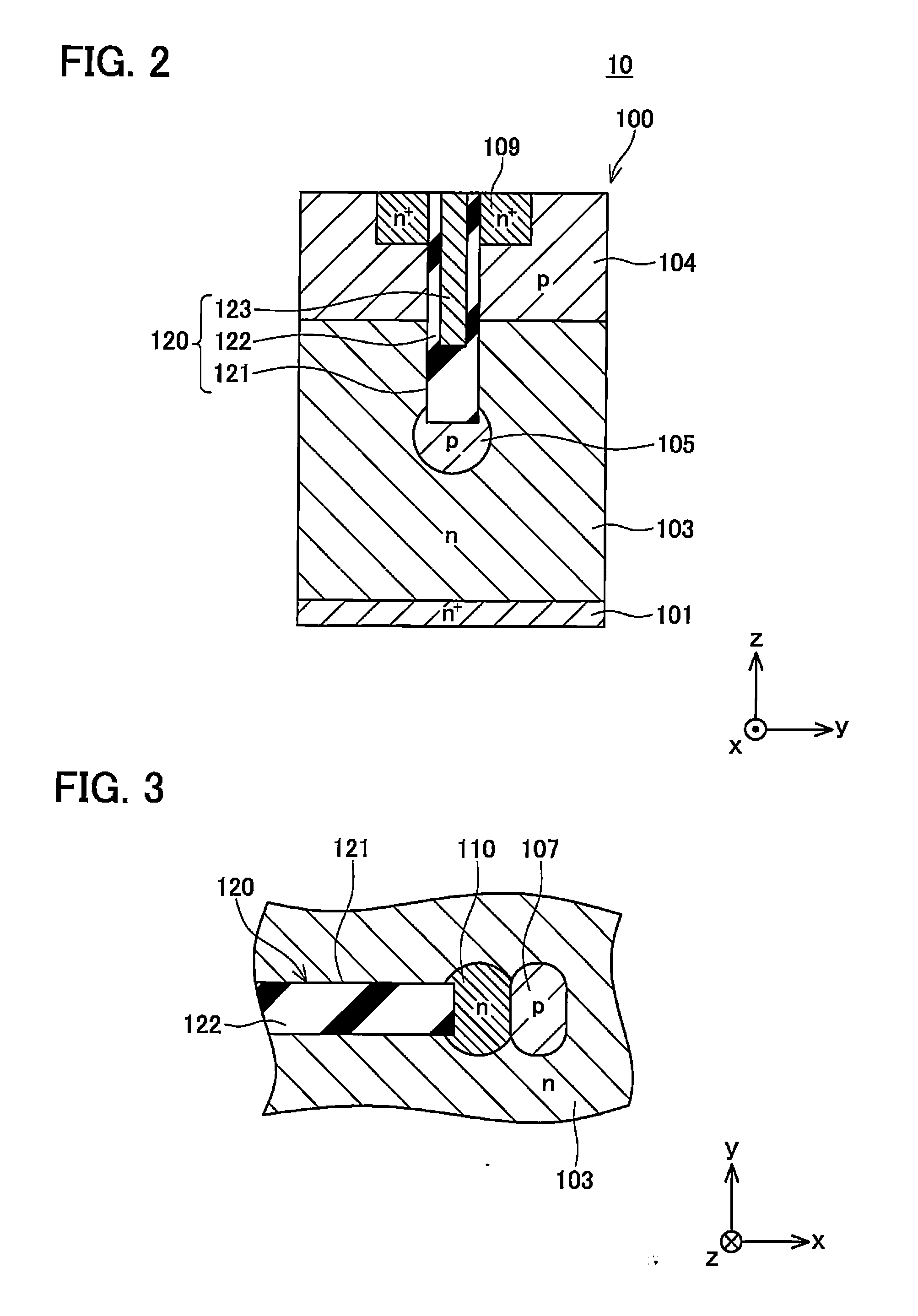
[0021]FIG. 1 shows a semiconductor device 10 according to a first embodiment. The semiconductor device 10 includes a semiconductor substrate 100, a trench gate 120 that is formed on an upper surface side of the semiconductor substrate 100 (a positive direction side of a z-axis), and peripheral trenches 130. The semiconductor substrate 100 is formed by silicon carbide.

[0022]A vertical MOSFET is formed in the semiconductor substrate 100. As shown in FIG. 1 and FIG. 2, the semiconductor substrate 100 includes an n-type drain layer 101, an n-type drift layer 103, a p-type body layer 104, an n-type source layer 109, a p-type first semiconductor layer 105, a p-type semiconductor layer 106, a p-type connecting layer 107, and an n-type second semiconductor layer 110. The body layer 104 is in contact with an upper surface of the drift layer 103, and a part of the body layer 104 is exposed on an upper surface of the semiconductor substrate 100. The source layer 109 is provided on a part of an...


PUM


Abstract

A semiconductor device includes a first semiconductor layer surrounding a bottom of the trench gate, a second semiconductor layer disposed along one of end portions of the trench gate in a longitudinal direction of the trench gate, one of end portions of the second semiconductor layer contacting the body layer and the other of the end portions of the second semiconductor layer contacting the first semiconductor layer, and a connecting layer, one of end portions of the connecting layer being connected to the body layer and the other of the end portions of the connecting layer being connected to the first semiconductor layer, the connecting layer contacting the second semiconductor layer, and the connecting layer being separated from the one of the end portions of the trench gate in the longitudinal direction of the trench gate by the second semiconductor layer.

Description

CROSS REFERENCE TO RELATED APPLICATION[0001]This is a national phase application based on the PCT International Patent Application No. PCT / JP2012 / 080159 filed on Nov. 21, 2012, the entire contents of which are incorporated herein by reference.TECHNICAL FIELD[0002]The present invention as described herein relates to a semiconductor device.BACKGROUND ART[0003]According to an insulated gate type semiconductor device for a power device, a high voltage and a low on-resistance generally have a trade-off relationship. A MOSFET having a floating structure at a bottom of a trench has the high voltage, but at the same time, it has a problem of deterioration in on-resistance property. In order to cope with this problem, Patent Document 1 provides a low concentration p-layer for connecting a p-type body layer and the floating structure at the bottom of the trench such that the low concentration p-layer comes in contact with end portions of the trench in a longitudinal direction of the trench. T...

Claims


Application Information

Patent Timeline
Patent Type & Authority Applications(United States)
IPC IPC(8): H01L29/78H01L29/10H01L29/08H01L29/423
CPCH01L29/7813H01L29/0878H01L29/1095H01L29/4236H01L29/0623H01L29/66734H01L29/1608H01L29/66068H01L21/047H01L29/0886H01L29/7809
Inventor SOENO, AKITAKAYAMAMOTO, TOSHIMASA
Owner TOYOTA JIDOSHA KK
Why Eureka
Try Eureka