Microlens array and method for fabricating thereof

a microlens array and array technology, applied in the field of microlens arrays, can solve the problems of viewer's eyes fatigue, viewer's dizziness, and inability to perform various functions depending on the purpose of a user on a single electronic device, and achieve the effect of reducing/enlargering a specific par

Active Publication Date: 2015-02-12
ELECTRONICS & TELECOMM RES INST
View PDF5 Cites 10 Cited by
  • Summary
  • Abstract
  • Description
  • Claims
  • Application Information

AI Technical Summary

Benefits of technology

[0017]The present disclosure also relates to a microlens array which is able to prevent display distortions and image switches between 2D and 3D, and a method for fabricating thereof.
[0029]In addition, according to the present disclosure, a lens shape can be implemented or a lens shape can be deformed into various shapes in real time through applying heat and voltage to the flexible thin layer so that it allows preventing display distortion during projection, being 2D / 3D image switchable, and providing selectively in a virtual display or in a 3D image at the same structure.
[0030]According to the present disclosure, a microlens shape can be deformed into various structures through applying heat and voltage so that it allows controlling a lens focal distance on the thin film structure and changing an optical angle without requiring an additional driving part.
[0032]For example, when the microlens of the present disclosure is used to an existing electronic devices or flexible electronic devices, it is able to provide flat panel display without distortion, regardless of the shape of the display surface during the projection, perform a variety of functions such as reduction / enlargement of a specific part on the display screen, and provide realistic 3D display to a flexible device through lens shape changes.

Problems solved by technology

However, since both technologies create 3D images with front perception of depth, there are technical limitations such that 3D images are significantly different depending on the viewing angle and it causes fatigue of viewer's eyes and dizziness of viewer.
However, such methods have still difficulties in manufacturing microlens array having ensured flexibility and desired material properties and further, since lens factors are fixed, it cannot perform various functions depending on the purpose of a user on a single electronic device.
It has some drawbacks such that it is hard to implement in a single layer structure since a shape is deformed by applying heat to a lens layer using a heat applying sheeting; it is difficult to control the focal distance of the lens more than one step since the lens shape is deformed in a flat shape only when the sheeting is heated to a temperature above the transition temperature (Tg); it is difficult to change optical properties of individual lens or a part of the lens on the microlens array; and it has a difficult structure to change optical angle among the optical properties.
In addition, since the lens shape is deformed only with heat application, there is limitation in terms of responding rate of the lens when heat transfer rate is considered.
Even though various shapes of lenses which provide 3D images can be prepared by varying arrangements of the mixture of the polymer and the liquid crystal according to electric signals, dynamic control in a lens shape which is prepared during the process is not possible since the polymer becomes hardened due to UV irradiation, and 2D / 3D display conversion becomes difficult.
However, it also has a drawback such that it does not allow dynamic control in a lens shape produced during the manufacturing process, resulting in difficulties in appropriate changes of lens factors.

Method used


Image

  • Microlens array and method for fabricating thereof
  • Microlens array and method for fabricating thereof
  • Microlens array and method for fabricating thereof

Examples


Embodiment Construction

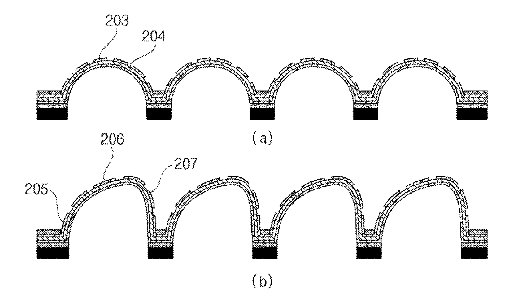
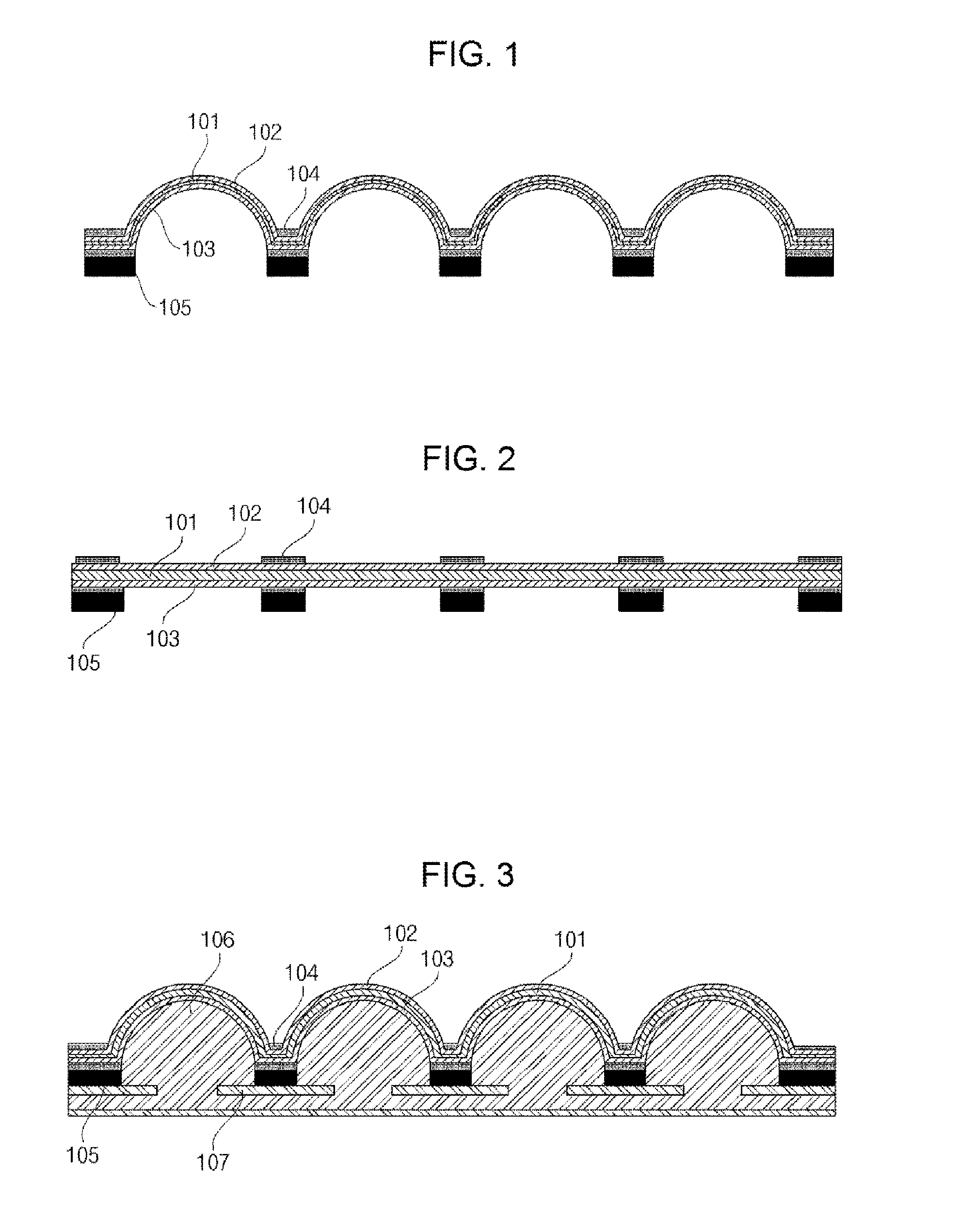
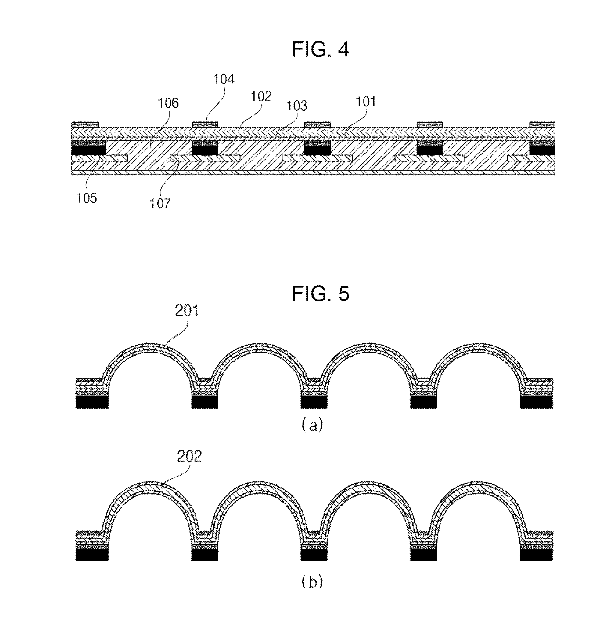
[0042]Hereinafter, a microlens array according to embodiments of the present invention and a method for fabricating the same will be described in detail with reference to the accompanying drawings. The necessary part to understand behaviors and functions according to the present invention will be described in more detail.

[0043]It will be understood that constitutional parts having identical names may be assigned with different reference numbers according to the Figures or assigned with identical reference numbers despite Figure numbers are different. However, it does not mean that each constitutional part has different characteristic function according to embodiments or has identical characteristic function in different embodiments so that the function of each constitutional part will be determined based on the description of each constitutional part in the corresponding embodiments.

[0044]The present disclosure is to provide a microlens array having variable optical properties by us...


PUM

PropertyMeasurementUnit
voltageaaaaaaaaaa
pressureaaaaaaaaaa
shapeaaaaaaaaaa

Abstract

A microlens array and a method for fabricating thereof are provided. The microlens array of the present invention comprises a lens structure part formed by bistable dielectric polymer thin film; first and second electrode parts each formed on the upper surface and the bottom surface of the lens structure part to apply voltage for shape changes of the lens structure part; a circuit part applying heat to the dielectric polymer thin film to change the property of the dielectric polymer thin film to be soft; and a base part formed on the bottom surface of the second electrode in predetermined intervals. The method further comprises a hydraulic part to apply predetermined voltage to the bottom surface of the lens structure part. The microlens array is thus able to change optical properties by deform the shape of a transparent dielectric polymer thin film having bistablity to various sizes of lens shapes by the purposes.

Description

CROSS-REFERENCE TO RELATED APPLICATIONS[0001]This application claims the benefit of Korean Patent Application No. 10-2013-0095215, filed with the Korean Intellectual Property Office on Aug. 12, 2013, the disclosure of which is incorporated herein by reference in its entirety.BACKGROUND[0002]1. Technical Field[0003]The present disclosure relates to a microlens array, more particularly to a microlens array which is able to change optical properties by deforming the shape of a transparent dielectric polymer thin film having bistablity to various sizes of lens shapes by the purposes, and a method for fabricating thereof.[0004]2. Background Art[0005]Not only high resolution screens but also virtual screens or 3D images have been provided with ongoing developments in display technologies which are used for mobile terminals, projectors and TVs that are currently available. Virtual screen technology uses a projection method based on a laser light source, a micromirror array, and a microlens...

Claims


Application Information

Patent Timeline
Patent Type & Authority Applications(United States)
IPC IPC(8): G02B27/22G02B26/08
CPCG02B26/0875G02B27/2214G02B3/0043G02B3/005Y10T29/49155G02B3/00G02B30/27
Inventor YUN, SUNG-RYULKYUNG, KI-UKPARK, SUN-TAKPARK, BONG-JENAM, SAE-KWANG
Owner ELECTRONICS & TELECOMM RES INST
Why Eureka
Try Eureka