Wireless power transfer through conductive materials

a technology of conductive materials and wires, applied in the direction of battery overheat protection, safety/protection circuits, transportation and packaging, etc., can solve the problems of significant limitations on the types of electric and electrical components, and the use of conductive materials in the vicinity of wireless power supplies

Active Publication Date: 2015-02-19
PHILIPS IP VENTURES BV
View PDF2 Cites 39 Cited by
  • Summary
  • Abstract
  • Description
  • Claims
  • Application Information

AI Technical Summary

Benefits of technology

[0016]In yet another aspect, the conductive material may be used to provide a surface with a metallic appearance for aesthetic purposes. The thin conductive material will allow electromagnetic fields to pass through the surface, but will still appear metallic. A hard top-coat may be applied over the conductive material to protect it from wearing away.

Problems solved by technology

One of the potential challenges faced by wireless power systems arises from the fact that electromagnetic fields interact with conductive materials.
Given the inherent nature of conductive materials, the use of conductive materials in an around wireless power supplies can be problematic.
Because conductive materials are an integral part of many electric and electrical components, these problems can place significant limitations on the types of electric and electrical components that can be situated in and around wireless power supplies, particularly in the electromagnetic field path between the primary coil and the remote device.

Method used


Image

  • Wireless power transfer through conductive materials
  • Wireless power transfer through conductive materials
  • Wireless power transfer through conductive materials

Examples


Embodiment Construction

I. Overview

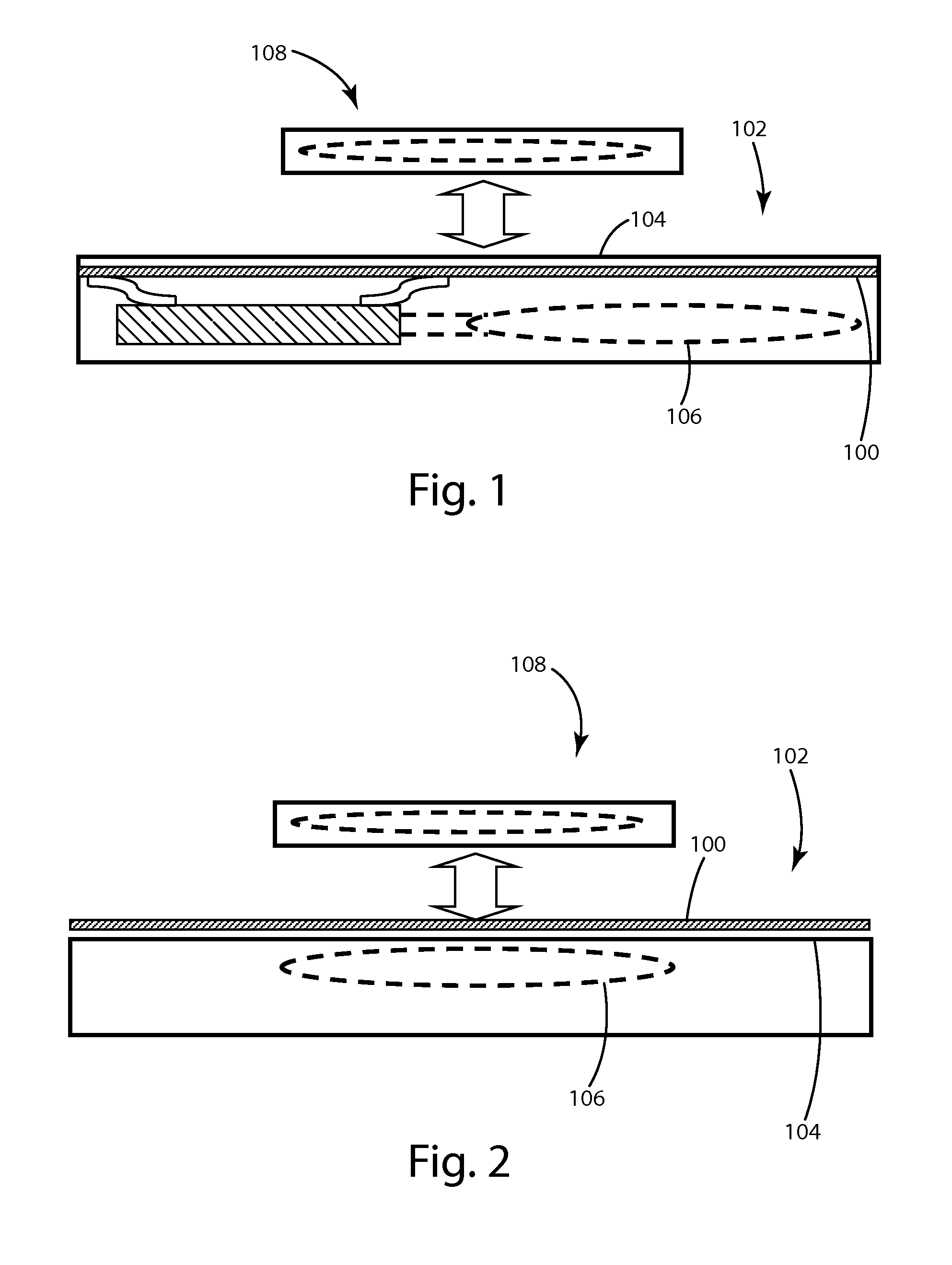
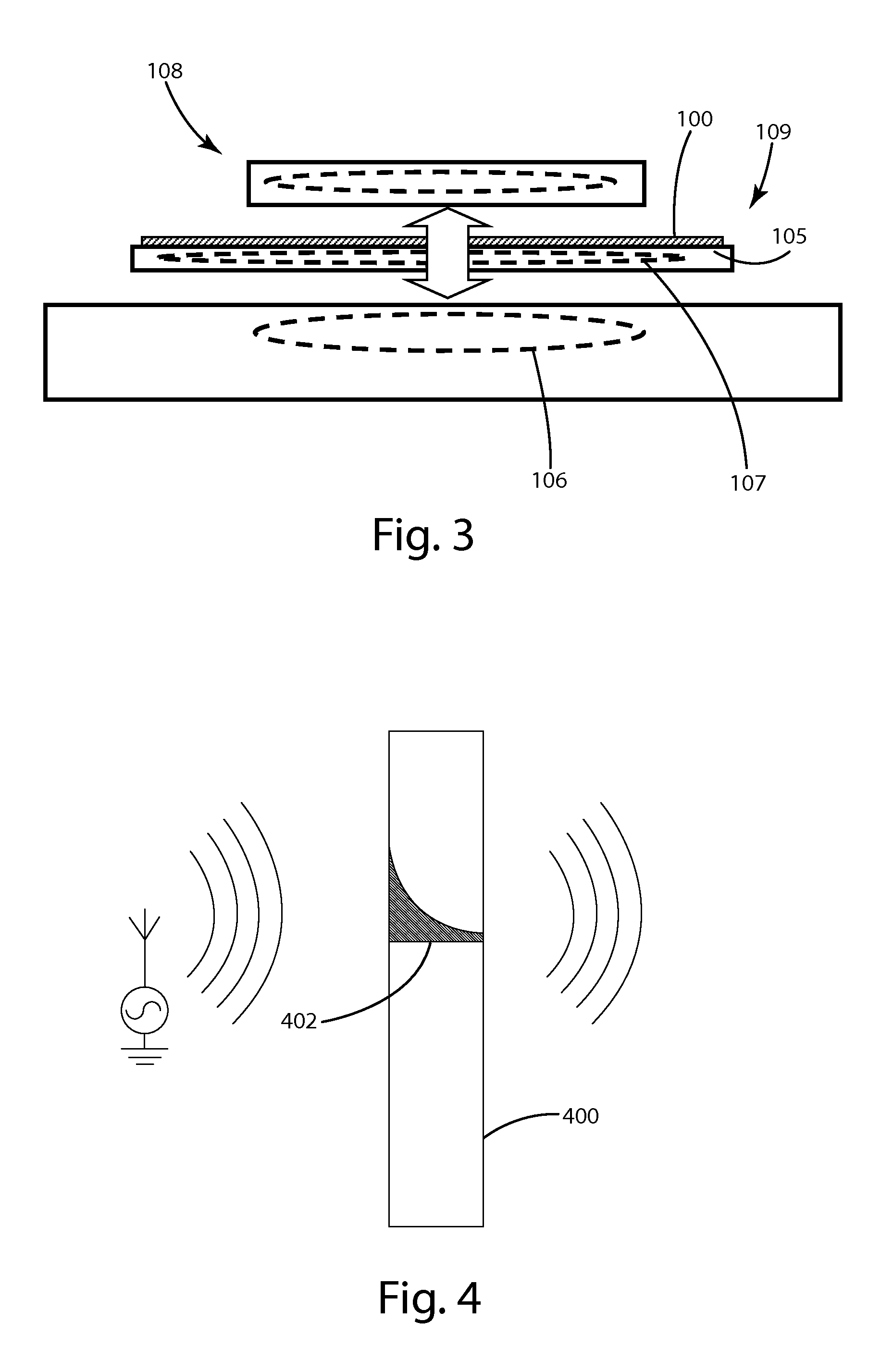
[0055]The present invention is generally directed to electrical components with conductive material incorporated into the electromagnetic field path of a wireless power system. The conductive material is configured to be sufficiently thin that it does not cause unacceptable heat gain or power loss when wireless power is being transferred. As schematically represented in FIGS. 1-3, the electrical components may be disposed in essentially any location within the flow path of the electromagnetic field from the wireless power supply to the remote device. For example, as shown in FIG. 1, the conductive material 100 may be disposed in a wireless power supply 102 below the power transfer surface 104. As another example, shown in FIG. 2, the conductive material 100 may be disposed above the power transfer surface 104 of the wireless power supply 102. In this embodiment, the conductive material 100 may be secured directly atop the power transfer surface 104 or may be separate and ...


PUM

PropertyMeasurementUnit
thickaaaaaaaaaa
temperatureaaaaaaaaaa

Abstract

An electrical component with conductive material(s) that is suitable for use within the electromagnetic field path of a wireless power transfer system. The electronic component includes conductive materials that are sufficiently thin to absorb no more than an acceptable amount of the electromagnetic field, yet thick enough to remain sufficiently conductive to perform the desired electrical function. In embodiments in which the wireless power supply delivers up to 20 watts of power, the conductive materials are not substantially thicker than about 1/10 the skin depth of the material at the anticipated wireless power frequency. The electrical component may be disposed at any location between the wireless power supply transmitter and the remote device receiver. The present invention permits the use of a wide rang of electrical components in the field path, such as a display, a sensor or a component capable of selectively operating as both.

Description

BACKGROUND OF THE INVENTION[0001]The present invention relates to the field of wireless power transfer, and more particularly to systems and methods of transferring wireless power through conductive metals.[0002]There has been a widespread increase in efforts to implement wireless power transfer systems in both commercial and residential settings. Wireless power systems offer the promise of eliminating power / charging cords for a wide range of electrically powered devices, including not only handheld electronics, such as cell phones, media players, wireless headsets and personal digital assistants, but also higher power devices, such as appliances, tools and electric vehicles. Inductive wireless power transfer systems use electromagnetic fields to transfer power from the power supply to the remote device without the need for wires or any direct electrical contact.[0003]In many applications, the wireless power supply includes a power transfer surface on which a remote device can be pl...

Claims


Application Information

Patent Timeline
Patent Type & Authority Applications(United States)
IPC IPC(8): H05K9/00H05B37/02H02J7/02H01F38/14H02J5/00
CPCH05K9/0049H01F38/14H05B37/0227H02J7/025H02J5/005H02J7/0044H05B47/115Y02B20/40H02J7/02H02J50/90H02J50/005H02J50/80H02J50/60H02J50/12H02J7/0047H02J7/00309H02J50/10
Inventor VAN DEN BRINK, JOSEPH C.NGUYEN, HAI D.MOES, BENJAMIN C.KUYVENHOVEN, NEIL W.
Owner PHILIPS IP VENTURES BV
Why Eureka
Try Eureka