
Power Source for Clock Distribution Network

a power source and clock technology, applied in the field of integrated circuits, can solve problems such as adversely affecting clock signals, and achieve the effect of reducing the amount of jitter and less susceptible to nois

Active Publication Date: 2015-02-19
APPLE INC
View PDF8 Cites 4 Cited by
  • Summary
  • Abstract
  • Description
  • Claims
  • Application Information

AI Technical Summary

Benefits of technology

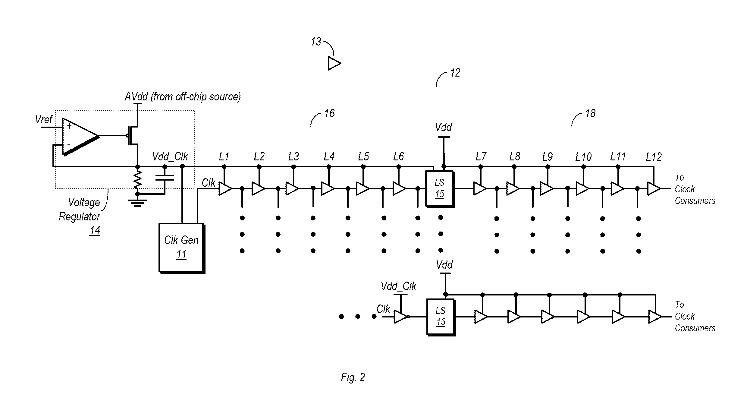
This patent aims to improve the performance of clock distribution networks in integrated circuits. It proposes a method to reduce jitter in the distributed clock signal, which can be achieved by implementing a separate power source for the buffers of the clock distribution network. This power source is less susceptible to noise, which can affect the quality of the clock signal. This separation of power sources can be achieved by using a separate power grid for the clock distribution network, which is different from the power grid used for logic circuits. Ultimately, this method improves the overall performance of clock distribution networks in integrated circuits.

Problems solved by technology

Jitter, an undesired deviation from true periodicity, is one factor that can adversely affect a clock signal.
If left unchecked, jitter can cause erroneous operation of synchronous circuits and may even cause them to fail.
Causes of jitter can include such factors as power supply noise, intrinsic device noise in the clock generator, and crosstalk with wires carrying other signals.

Method used


Image

  • Power Source for Clock Distribution Network
  • Power Source for Clock Distribution Network
  • Power Source for Clock Distribution Network

Examples


Embodiment Construction

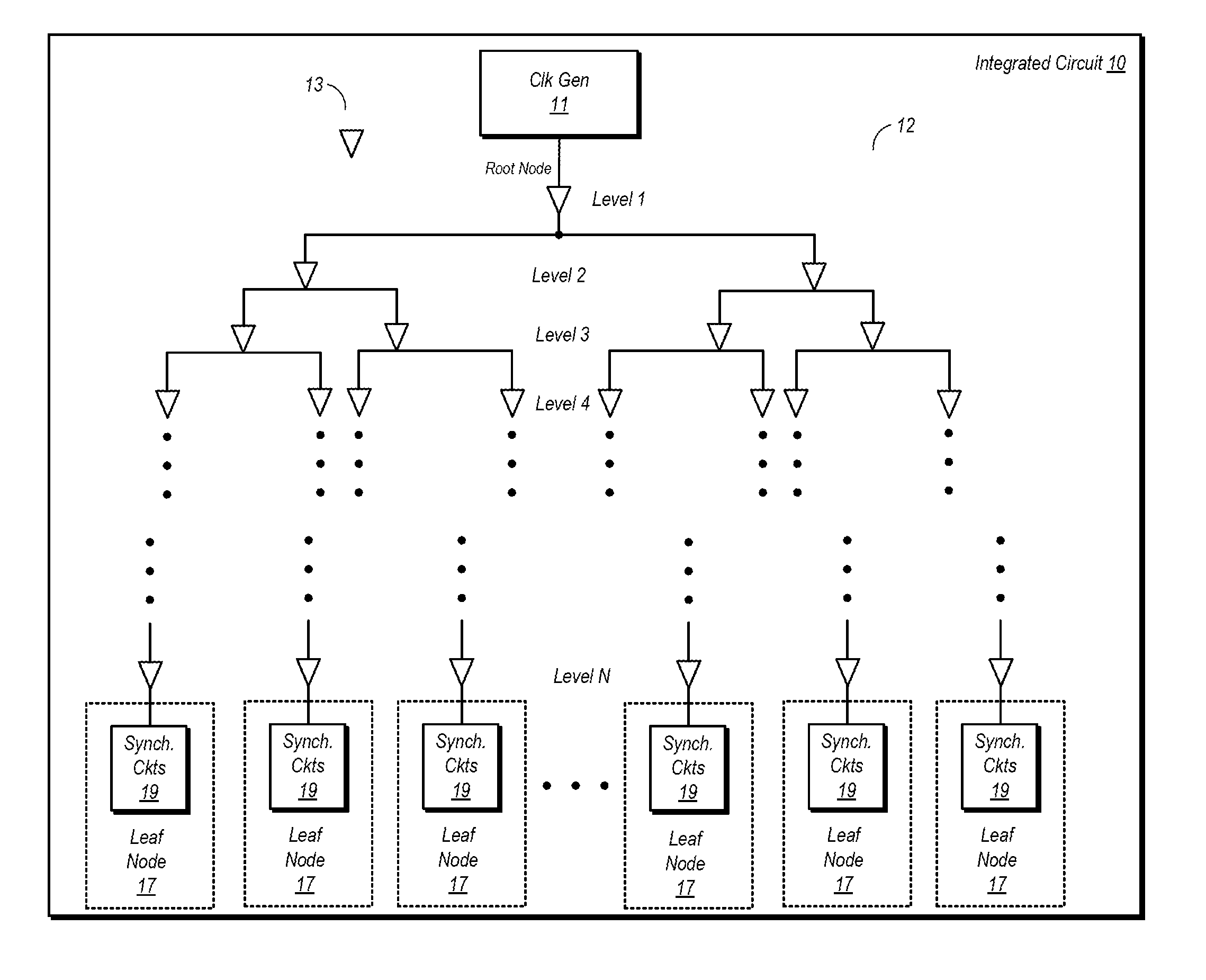
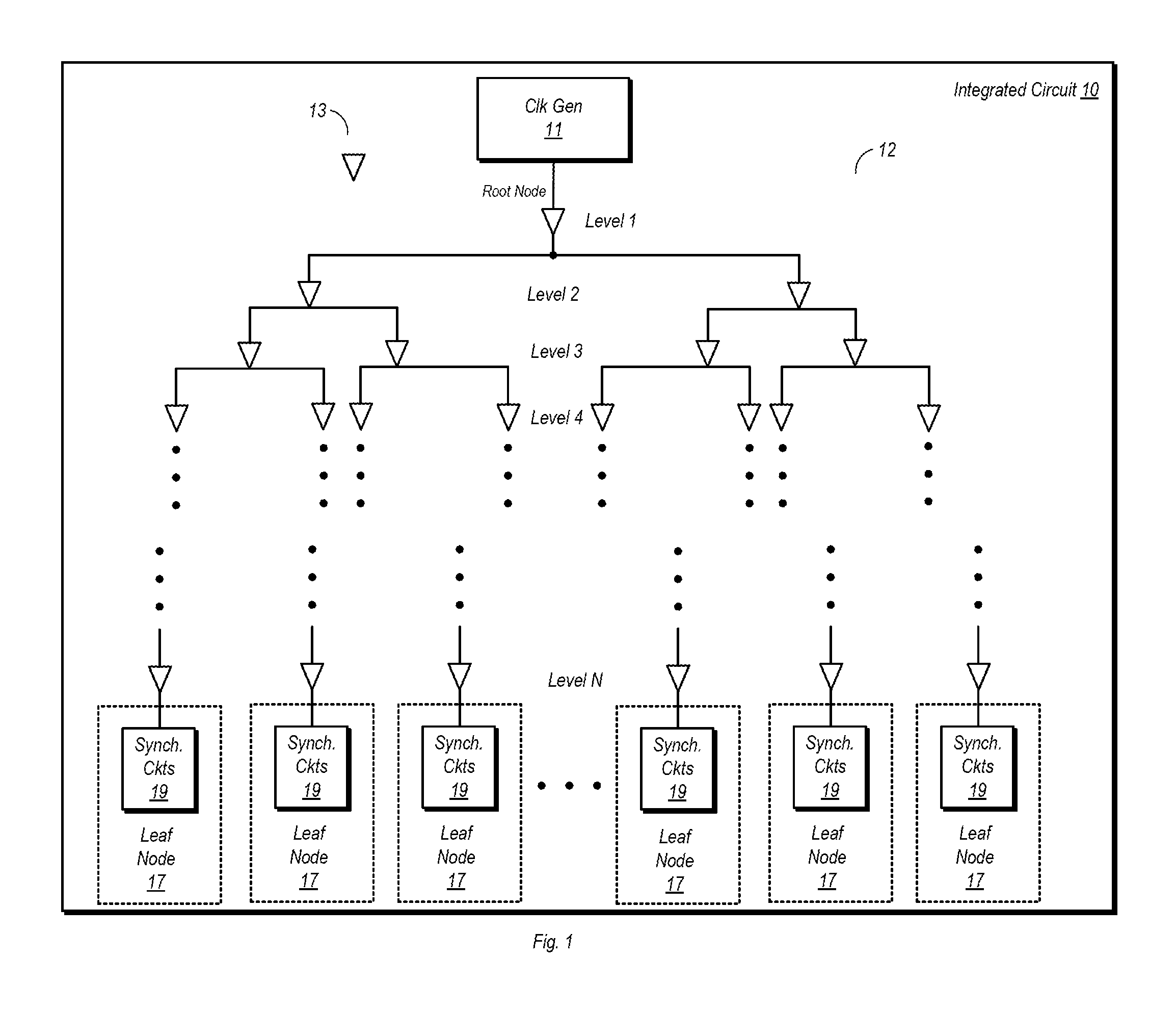
[0018]FIG. 1 is a block diagram of one embodiment of an integrated circuit including a clock distribution network. In the embodiment shown, integrated circuit (IC) 10 includes a clock generation circuit 11 that is configured to generate a clock signal for distribution to a number of different synchronous circuit 19. Clock generation circuit 11 may be one of a number of different types of clock generation circuits, such as an oscillator, a phase locked loop (PLL) or any other circuit capable of generating a clock signal. The synchronous circuits 19 may be any type of circuitry that utilizes one or more clock signals during operation. Such clock consumer circuits include, but are not limited to, flip-flops, timers, execution units, or any other sequential logic circuits. Each instance of synchronous circuits 19 shown in FIG. 1 may represent one or more circuits that utilize the clock signal. For example, a block of synchronous circuits 19 may represent a group of flip-flops, a single ...


PUM


Abstract

A clock distribution network having a separate power supply for top levels thereof is disclosed. In one embodiment, an integrated circuit includes a clock distribution network configured to distribute a clock signal to each of a number of clock consumers. The clock distribution network is arranged in a hierarchy of levels, with each of the levels including at least one buffer, and with the upper levels being closer to a source of the clock signal and the lower levels being closer to the clock consumers. The buffers of the upper levels are coupled to receive power from a first power source, via a first power grid. The buffers of the lower levels are coupled to receive power from a second power source, separate from the first, via a second power grid.

Description

BACKGROUND[0001]1. Technical Field[0002]This disclosure is directed to integrated circuits, and more particularly, to networks for distributing a clock signal in an integrated circuit.[0003]2. Description of the Related Art[0004]Modern digital integrated circuits use clock signals to synchronize the operation of sequential circuits implemented therein. A given clock signal may be provided to a number of circuits (e.g., flip-flops) within a corresponding clock domain. Since the number of circuits utilizing the clock signal may be large and relatively remote from the clock source, a clock distribution network (sometimes referred to as a ‘clock tree’) may be used to distribute the clock signal. A clock tree may include a number of levels, with buffers implemented at the various levels. At a node known as a root node of the clock tree, the clock signal may be received by a buffer from a clock source. The buffer may distribute the clock signal to additional buffers of the next level of t...

Claims


Application Information

Patent Timeline
Patent Type & Authority Applications(United States)
IPC IPC(8): H03K3/012
CPCH03K3/012G06F1/10
Inventor KUMAR, ROHIT
Owner APPLE INC
Learn More