Photoelectric converting apparatus

a technology of photoelectric conversion and conversion apparatus, which is applied in the field can solve the problems of difficult construction of photoelectric conversion apparatus of a high sensitivity, significant decrease in output voltage, and inability to construct prior photoelectric conversion apparatus such as the radiation image pickup apparatus into a large area, etc., and achieves low electric power consumption, simple configuration, and reduced noise

Inactive Publication Date: 2009-09-22
CANON KK
View PDF25 Cites 12 Cited by
  • Summary
  • Abstract
  • Description
  • Claims
  • Application Information

AI Technical Summary

Benefits of technology

[0014]An object of the present invention is to provide a photoelectric converting apparatus capable of reducing the influence of noise resulting from a parasitic capacitance, and readable with a readout circuit of a simple configuration with a low electric power consumption.
[0018]According to the present invention, it is possible, even in a sensor of a large area, to suppress a loss in the output voltage resulting from an increase in the parasitic capacitance. Therefore the sensor is less susceptible to the influence of noise, and can provide a high sensitivity. Also a readout means can be constructed without employing a special circuit such as a low-noise amplifier or a special constant current source. Also a readout means can be constructed with low electric power consumption and with little troublesome heat generation. Furthermore, the constant current source employed in the present invention can be formed by a thin film transistor on a glass substrate. Therefore, it can be formed by means of film formations simultaneously with the photoelectric converting element and other thin film transistors, thus being advantageous in cost. Also the constant current source can be provided in a distant location from the readout means on the glass substrate, thereby alleviating the influence of the resistance of the signal line.

Problems solved by technology

However, in the prior photoelectric converting apparatus such as the radiation image pickup apparatus, a large parasitic capacitance is generated in the common signal line as the number of pixels arranged two-dimensionally increases, thus leading to a significant decrease in the output voltage.
Therefore, the prior photoelectric converting apparatus such as the radiation image pickup apparatus cannot be constructed into a sensor of a large area because of this significant loss in the output voltage.
Also because of this loss in the output voltage, such apparatus is susceptible to the influence of noise generated in the amplifiers of the readout circuit and of external noise, whereby a photoelectric converting apparatus of a high sensitivity may be difficult to construct.
The influence of such noise may be reduced by providing the readout circuit with a constant current power source or low-noise amplifiers, but such low-noise amplifier, being a special circuit, leads to drawbacks such as an increased cost.
Also, since such low-noise amplifier generally has a high electric power consumption, the readout circuit will cause non-negligible heat generation.

Method used


Image

  • Photoelectric converting apparatus
  • Photoelectric converting apparatus
  • Photoelectric converting apparatus

Examples


first embodiment

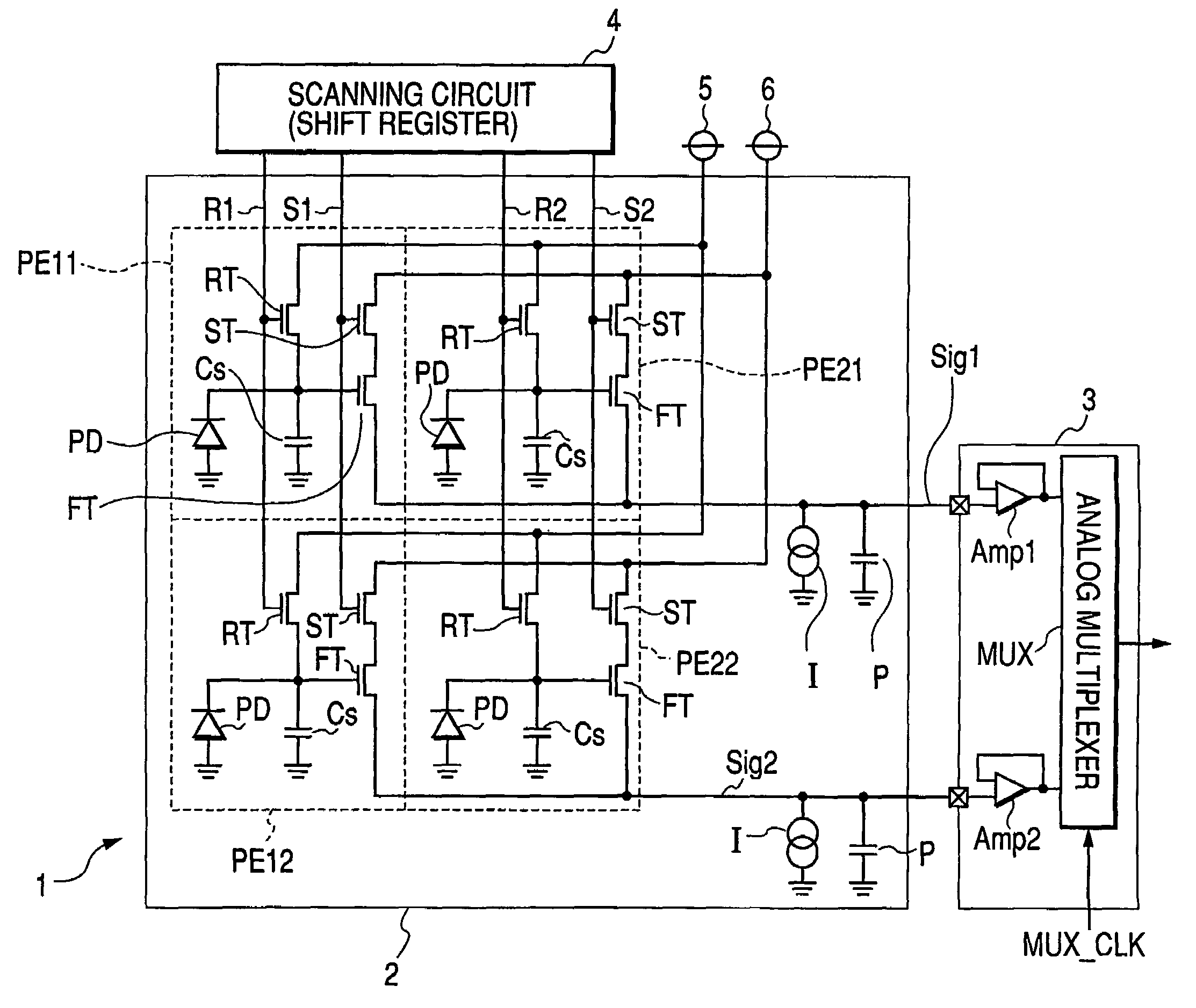
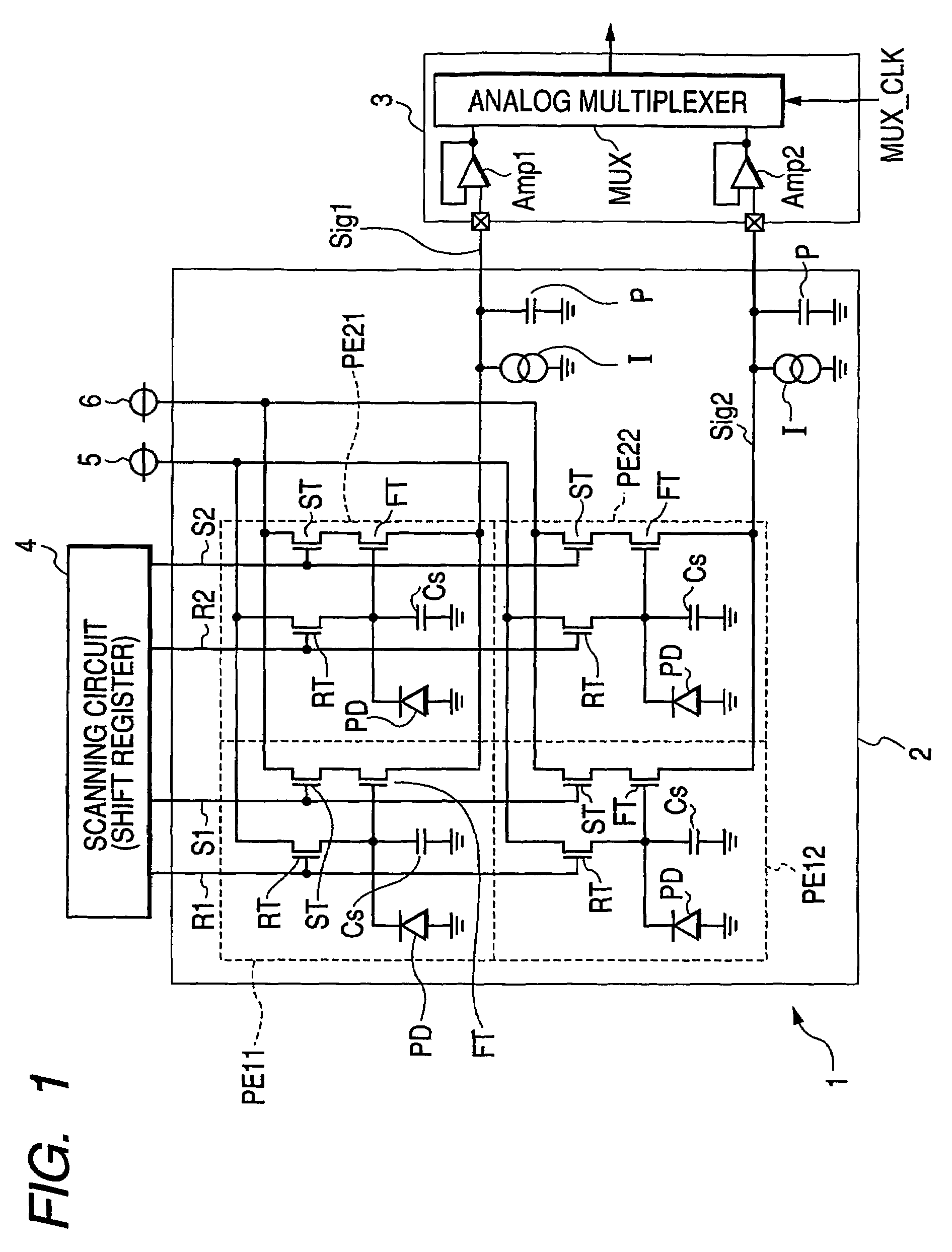
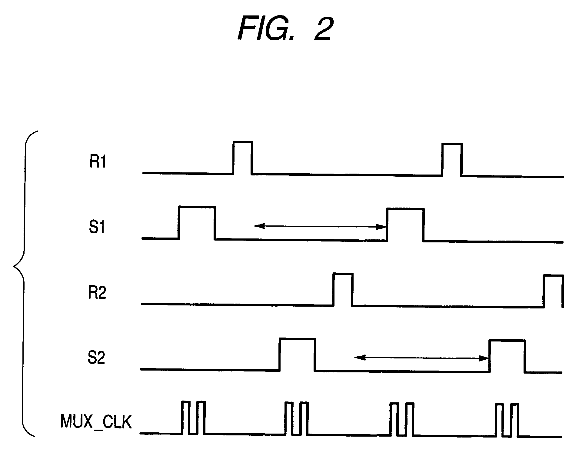
[0040]At first there will be explained a first embodiment of the present invention. FIG. 1 is a circuit diagram showing a circuit structure of a photoelectric converting apparatus, particularly an X-ray image pickup apparatus, constituting the first embodiment of the present invention.

[0041]In the present embodiment, a sensor array 1 is constructed on a glass substrate 2, by arranging four pixels PE11, PE12, PE21 and PE22 in two rows and two columns, but the number of pixels constituting the sensor array 1 is not limited to such example. Each pixel is provided with a photoelectric converting element PD constituted of a PIN photodiode formed with amorphous silicon, and a storage capacitance Cs for accumulating a signal charge generated by the photoelectric converting element PD. The photoelectric converting element PD and the storage capacitance Cs are grounded at one terminal thereof and are mutually connected at their other terminal. Each pixel is further provided with a resetting ...

second embodiment

[0052]In the following, there will be explained a second embodiment of the present invention. FIG. 3 is a circuit diagram showing a circuit structure of a photoelectric converting apparatus, particularly an X-ray image pickup apparatus, constituting a second embodiment of the present invention. In the second embodiment, in place for the constant current source I employed in the first embodiment, a thin film transistor (TFT) CT formed by amorphous silicon is provided. A gate of the thin film transistor CT receives a voltage from a power supply 7 for a constant current source. Such structure can be produced by a simple manufacturing process, as the constant current source can be simultaneously formed by means of film formations with other transistors (resetting, selecting and source follower). The thin film transistors for resetting, for selecting, for source follower and for constant current source may have same laminated film thicknesses or individually different film thicknesses. T...

third embodiment

[0057]In the following, there will be explained a third embodiment of the present invention. FIG. 5 is a circuit diagram showing a circuit structure of a photoelectric converting apparatus, particularly an X-ray image pickup apparatus, constituting a third embodiment of the present invention. In contrast to the second embodiment, in which the thin film transistor CT constituting the constant current source is positioned between a pixel and the readout circuit 3, in the third embodiment, the thin film transistor CT is located, on the common signal line, at a position more spaced from the readout circuit 3 than the pixel. Stated differently, the pixel is positioned between the thin film transistor CT and the readout circuit 3.

[0058]An advantage of a spaced arrangement of the constant current source from the readout circuit will be explained with reference to FIGS. 15, 16 and 17.

[0059]FIG. 15 shows a structure in which, for each signal line, the constant current source is spaced from t...


PUM


Abstract

A photoelectric converting apparatus of the present invention includes, in one embodiment, a photoelectric converting element, a resetting transistor in which a source is connected to the photoelectric converting element and a drain is connected to a resetting power source, a readout transistor in which a gate is connected to the photoelectric converting element and a drain is connected to a readout power source, a signal line connected to a source of the readout transistor, a selecting transistor connected between the readout power source or the signal line and the readout transistor, and a constant current source connected to the signal line.

Description

RELATED APPLICATIONS[0001]This application claims priority from Japanese Patent Applications Nos. 2003-389274, filed on Nov. 19, 2003, and 2004-180899, filed on Jun. 18, 2004, which are hereby incorporated by reference herein.TECHNICAL FIELD[0002]The present invention relates to a photoelectric converting apparatus such as a radiation image pickup apparatus, and more particularly to a photoelectric converting apparatus designed for reducing sensitivity loss resulting from a parasitic capacitance.BACKGROUND ART[0003]There is already known a photoelectric converting apparatus such as a radiation image pickup apparatus which reads a charge produced by photoelectric conversion in a photoelectric converting element of a sensor array utilizing amorphous silicon or polysilicon, by transfer of the charge to a capacitance by means of a matrix drive.[0004]FIG. 9 is a schematic circuit diagram showing a prior photoelectric converting apparatus (radiation image pickup apparatus). In the prior p...

Claims


Application Information

Patent Timeline
Patent Type & Authority Patents(United States)
IPC IPC(8): H01L27/146A61B6/00G01T1/20G01T1/24H01L27/14H01L31/09H04N5/32H04N5/335H04N5/357H04N5/369H04N5/374
CPCH01L27/14658H04N5/32H04N5/378H04N5/374H04N5/3658H04N25/677H04N25/76H04N25/75
Inventor KAMESHIMA, TOSHIO
Owner CANON KK
Why Eureka
Try Eureka