Liquid crystal display device and driving method thereof

a technology of liquid crystal display and driving method, which is applied in the direction of electric digital data processing, instruments, computing, etc., can solve the problems of optimum common voltage generation, flickering, and large off-leak current flowing at a time of the off state, and achieve the effect of increasing the amount of electric charges accumulated in the pixel capacitance and reducing the amount of electric charges

Active Publication Date: 2015-02-19
SHARP KK
View PDF3 Cites 9 Cited by
  • Summary
  • Abstract
  • Description
  • Claims
  • Application Information

AI Technical Summary

Benefits of technology

[0019]In accordance with the first aspect, when the off-sequence control circuit applies the scanning signal with the first level by the fact that the liquid crystal display device shifts to the off-sequence mode, the off-sequence control circuit supplies to each of the signal lines the data signal with the potential corresponding to the shift amount of each of the image signals, the shift amount being determined by the level difference between the first level and the second level, the parasitic capacitance formed between the gate terminal and drain terminal of the thin film transistor, and the synthetic capacitance of the pixel formation portion including the parasitic capacitance. In this way, the data signal supplied to the signal line is written into the pixel formation portion. Next, the scanning signal is turned to the ground potential, whereby the potential of the written data signal is shifted and cancelled owing to a coupling effect by the parasitic capacitance. As a result, a voltage applied to the liquid crystal layer of the pixel formation portion becomes 0V, and accordingly, the afterimage owing to the image persistence of the liquid crystal and the flicker owing to the deviation of the optimum common voltage can be prevented from occurring.
[0020]In accordance with the second aspect, the first level of the scanning signal is set at the level between the level necessary to turn the thin film transistor to the on state in the on-sequence mode and the ground potential. In this way, even in a case where a capacitance value of the liquid crystal capacitance is varied because of process variations of the liquid crystal panel, the first level of the scanning signal is reduced, whereby the potential of the data signal at the time of the off sequence can be set at a value more approximate to the ground potential. Therefore, it becomes unnecessary to set different values as the potential of the data signal for each of the liquid crystal panels, and accordingly, it becomes easy to set the potential of the data signal. Moreover, an amount of electric charges accumulated in the pixel capacitance is further reduced, and accordingly, the direct current voltage applied to the liquid crystal layer can be set at 0V in a short time by leakage through the liquid crystal layer and the thin film transistor.
[0021]In accordance with the third aspect, the first level of the scanning signal is set at the plurality of levels set in a level order, and the scanning signals different in level at the time of the off sequence can be applied to the scanning line in a level order. In this way, the data signal at the time of the off sequence, which is supplied to the signal line, can be surely written into the pixel formation portion. Therefore, when the scanning signal with the ground potential is applied, the direct current voltage applied to the liquid crystal layer can be surely set at 0V.
[0022]In accordance with the fourth aspect, when the scanning signal with the first level of the scanning signal in the off sequence mode is applied to the gate terminal of the thin film transistor, a predetermined period for applying the scanning signal with the first level to the scanning line is lengthened as the on current is smaller. In this way, the data signal at the time of the off sequence, which is supplied to the signal line, can be surely written into the pixel formation portion.
[0023]In accordance with the fifth aspect, the first level of the scanning signal at the time of the off sequence is the same level as the level necessary to turn the thin film transistor to the on state in the on-sequence mode. In this way, the value of the voltage applied to the gate terminal of the thin film transistor becomes high, and the on current is increased.
[0024]Therefore, the data signal supplied to the signal line at the time of the off-sequence mode can be written into the pixel formation portion in a short time, and accordingly, a time until the direct current voltage applied to the liquid crystal layer is set at 0V can be shortened.

Problems solved by technology

However, in a TFT having a channel layer made of amorphous silicon (a-Si) or continuous grain silicon (CGS silicon), an off-leak current that flows at a time of the off state is relatively large.
In this way, there occur such problems that the afterimage owing to the image persistence of the liquid crystal is generated, and that a flicker owing to deviation of an optimum common voltage is generated.

Method used


Image

  • Liquid crystal display device and driving method thereof
  • Liquid crystal display device and driving method thereof
  • Liquid crystal display device and driving method thereof

Examples


first embodiment

2. First Embodiment

[0044]

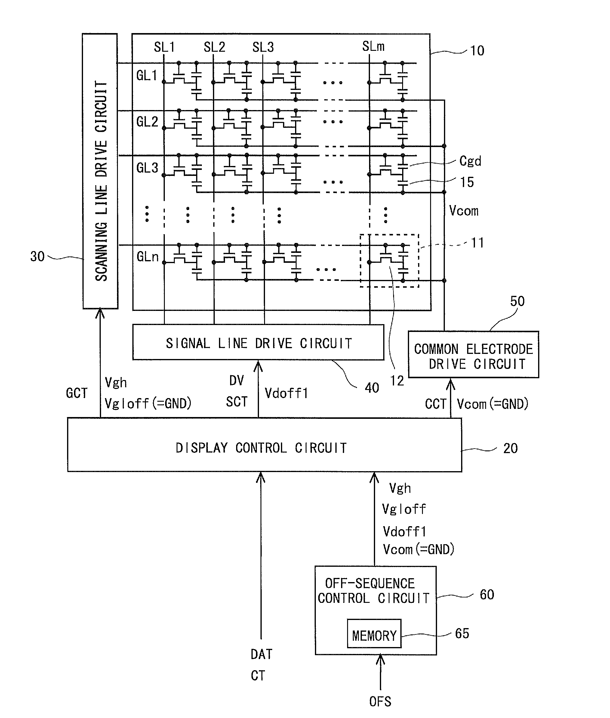
[0045]FIG. 4 is a block diagram showing a configuration of a liquid crystal display device according to a first embodiment of the present invention. As shown in FIG. 4, the liquid crystal display device includes: a display unit 10; a display control circuit 20; a scanning line drive circuit 30; a signal line drive circuit 40; a common electrode drive circuit 50; and an off-sequence control circuit 60. All of these units are formed on a liquid crystal panel (not shown) composed of an insulating substrate such as a glass substrate.

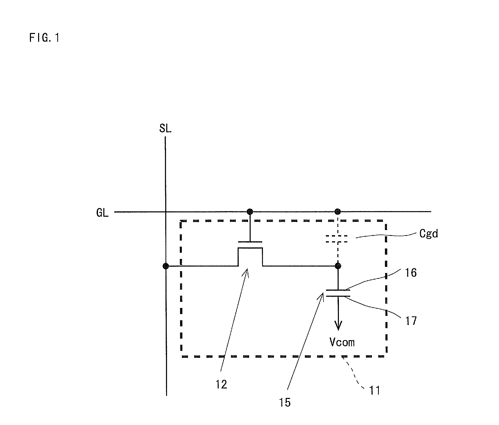
[0046]On the display unit 10, there are formed: a plurality (m) of signal lines SL1 to SLm; a plurality (n) of scanning lines GL1 to GLn; and a plurality (m×n) of pixel formation portions 11 provided so as to correspond to intersections of the m signal lines SL1 to SLm and the n scanning lines GL1 to GLn. Hereinafter, in a case where the m signal lines SL1 to SLm are not distinguished from one another, these are simply referred to as...

second embodiment

3. Second Embodiment

[0070]

[0071]A configuration of a liquid crystal display device according to a second embodiment is the same as the configuration of the liquid crystal display device according to the first embodiment, and accordingly, a block diagram showing the configuration is omitted. Moreover, among constituent elements included in the liquid crystal display device according to this embodiment, those different from the constituent elements included in the liquid crystal display device according to the first embodiment are mainly described.

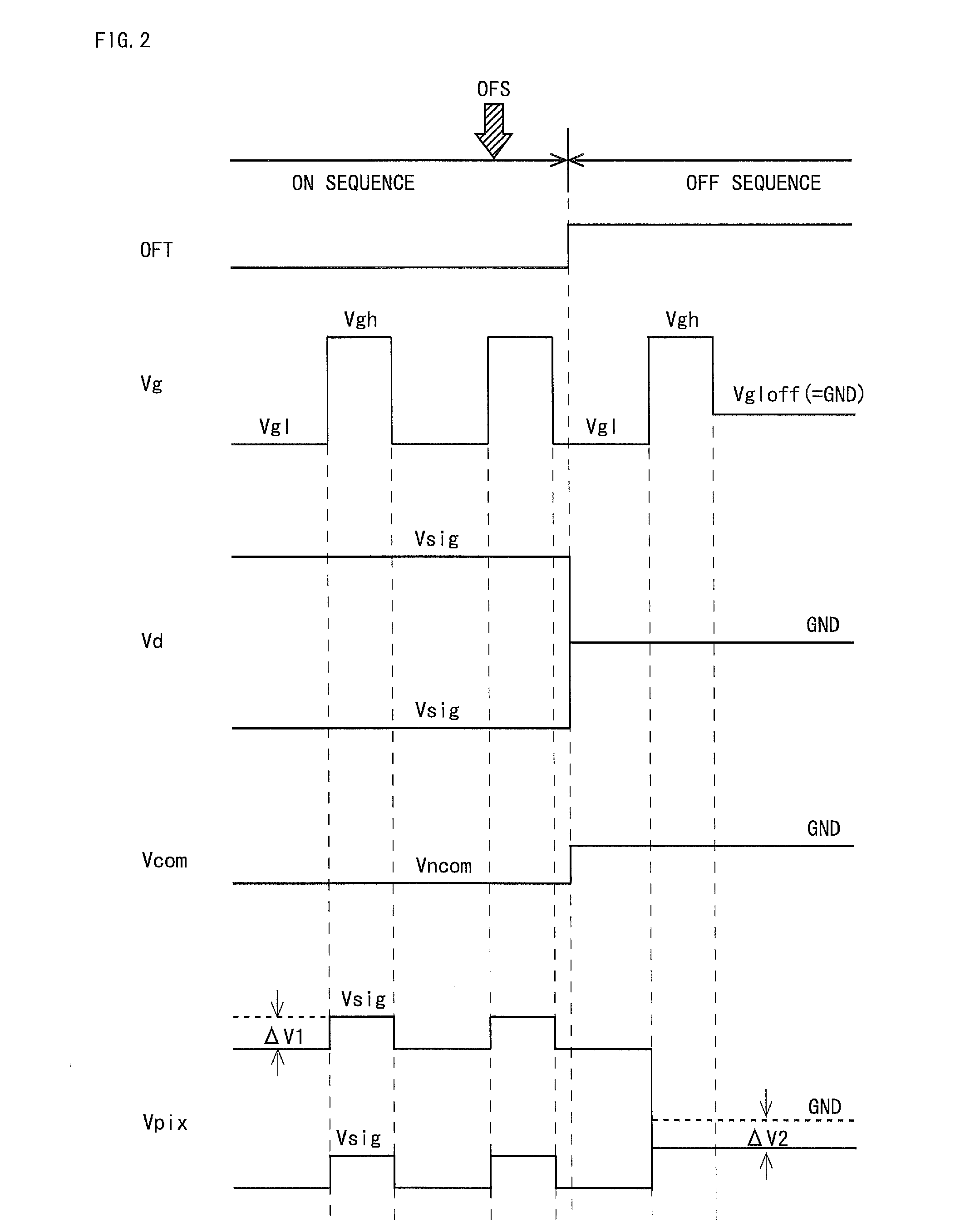
[0072]Operations of the respective circuits in the on-sequence mode are the same as those in the case of the first embodiment, and accordingly, a description thereof is omitted, and operations of the respective circuits in the off-sequence mode are described. In a case where the off signal OFS is given to the off-sequence control circuit 60, the off-sequence control circuit 60 reads out a variety of signals prestored in the memory 65, and ou...

third embodiment

4. Third Embodiment

[0088]

[0089]A configuration of a liquid crystal display device according to a third embodiment is the same as the configuration of the liquid crystal display device according to the first embodiment, and accordingly, a block diagram showing that configuration is omitted. Moreover, among constituent elements included in the liquid crystal display device according to this embodiment, those in which functions are different from those of the constituent elements included in the liquid crystal display device according to the first embodiment are mainly described.

[0090]Operations of the respective circuits in the on-sequence mode are the same as those in the case of the first embodiment, and accordingly, a description thereof is omitted, and operations of the respective circuits in the off-sequence mode are described. In a case where the off signal OFS is given to the off-sequence control circuit 60, the off-sequence control circuit 60 reads out a variety of signals pre...


PUM


Abstract

Provided are: a liquid crystal display device capable of rapidly discharging an image signal which is held in a pixel formation portion, when a power supply thereof is turned off; and a driving method of the liquid crystal display device. If the liquid crystal display device shifts to an off-sequence mode, then a data signal Vd with a potential Vdoff1 corresponding to a shift amount ΔV3 lowered by a coupling effect of a parasitic capacitance formed between a gate terminal and drain terminal of a thin film transistor (12) is applied to a signal line SL. When a scanning signal Vg turns to a high level, the data signal Vd applied to the signal line SL is written into the pixel formation portion (11), and a potential of a pixel signal Vpix becomes the Vdoff1. When the scanning signal Vg falls to a ground potential GND after an elapse of a period t1, the potential of the pixel signal Vpix is lowered by a shift amount ΔV3, and accordingly, the potential of the pixel signal Vpix becomes the ground potential GND. In this way, a direct current voltage applied to the liquid crystal layer also becomes 0V.

Description

TECHNICAL FIELD[0001]The present invention relates to a liquid crystal display device and a driving method thereof, and particularly, relates to an active matrix-type liquid crystal display device that shifts to an off-sequence mode in such a manner that a power supply is turned off, and to a driving method thereof.BACKGROUND ART[0002]On a display unit of an active matrix-type liquid crystal display device, a plurality of pixel formation portions are arranged in a matrix. On the respective pixel formation portions, thin film transistors (hereinafter, referred to as “TFTs”) which operate as switching elements are provided. By switching on / off the TFTs, driving image signals (hereinafter, referred to as “image signals”) for displaying an image are written into the pixel formation portions. The image signals are applied to liquid crystal layers of the pixel formation portions, and change orientation directions of liquid crystal molecules to directions corresponding to voltage values of...

Claims


Application Information

Patent Timeline
Patent Type & Authority Applications(United States)
IPC IPC(8): G09G3/36
CPCG09G3/3648G09G2330/022G09G2300/0871G09G2310/0289G09G2310/0251G09G2310/061G09G2320/0204G09G2320/0247G09G2320/0257G09G2330/027
Inventor KANEKO, SEIJI
Owner SHARP KK
Why Eureka
Try Eureka