Photodetector

a technology of photodetector and photoelectric field, which is applied in the direction of electrical apparatus, nanotechnology, semiconductor devices, etc., can solve the problems of cumbersome use of photodetector, and achieve the effect of widening the sensitive wavelength band

Inactive Publication Date: 2015-02-26
HAMAMATSU PHOTONICS KK
View PDF6 Cites 11 Cited by
  • Summary
  • Abstract
  • Description
  • Claims
  • Application Information

AI Technical Summary

Benefits of technology

[0029]The present invention can provide a photodetector which can detect light having no electric field component i

Problems solved by technology

When detecting a planar wave having a wavefront perpendicular to an advancing direction of light, for example, it is necessary for the light to be i

Method used


Image

  • Photodetector
  • Photodetector
  • Photodetector

Examples


first embodiment

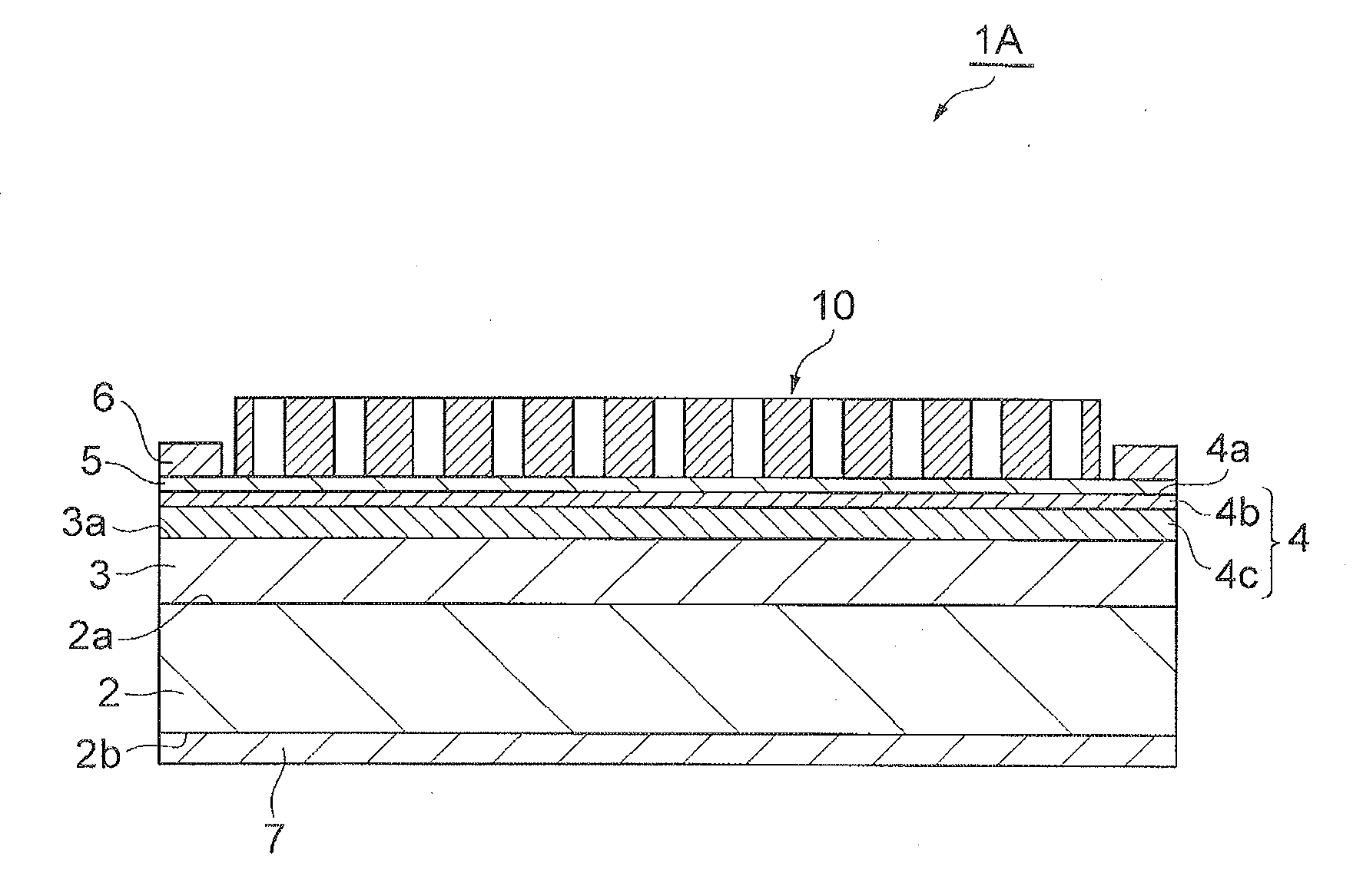
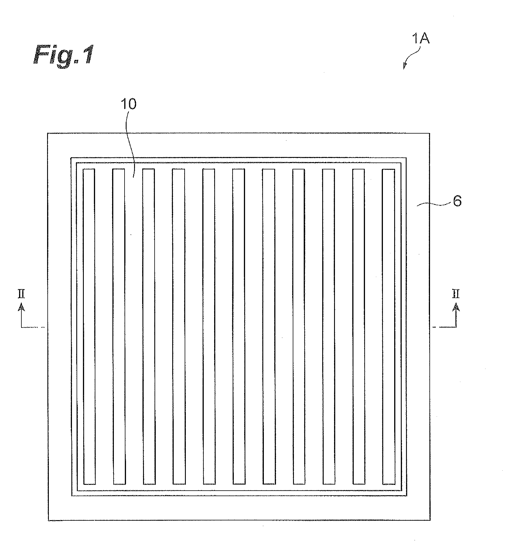
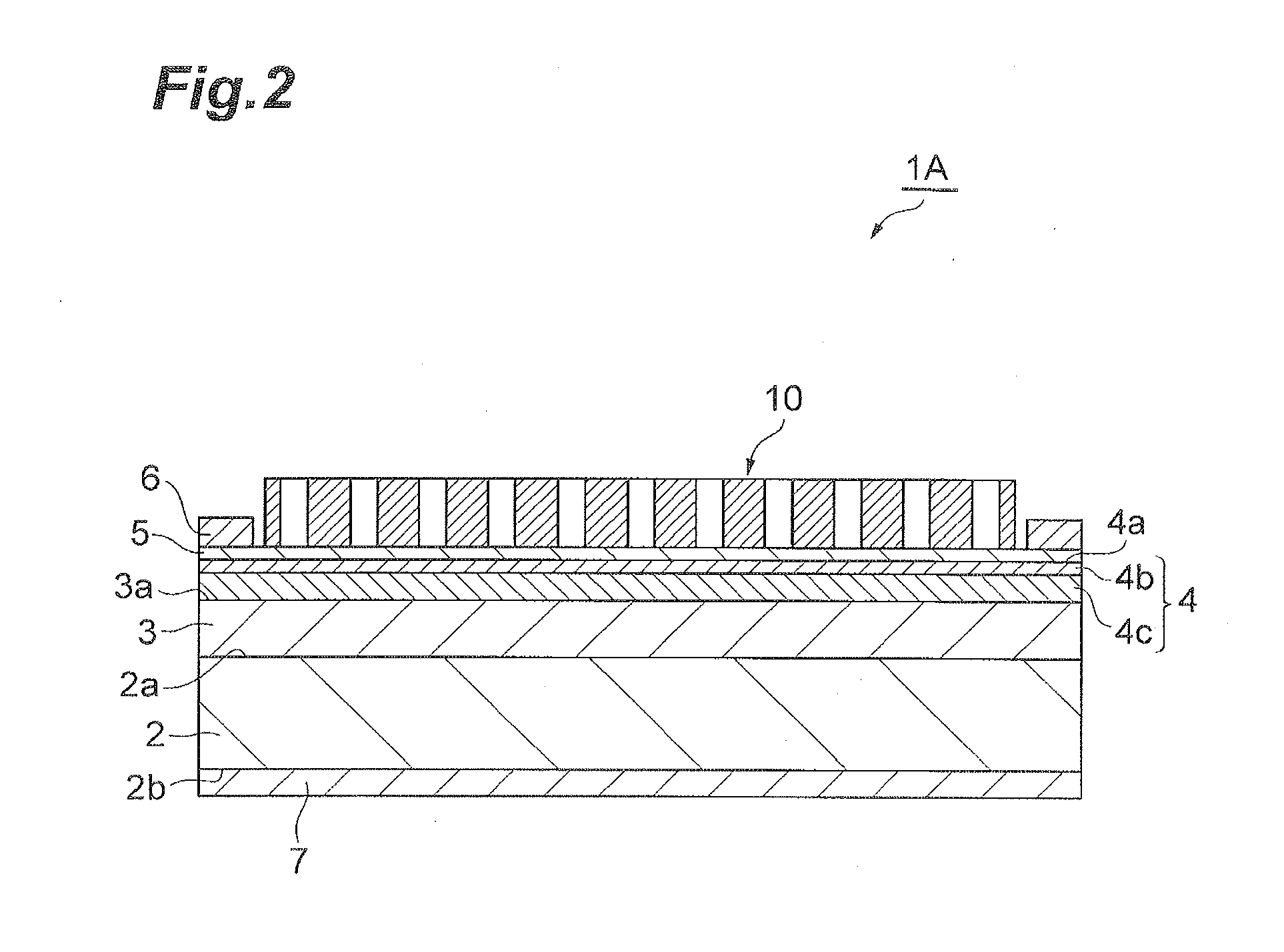
[0049]As illustrated in FIGS. 1 and 2, a photodetector 1A comprises a rectangular plate-shaped substrate 2 made of n-type InP having a thickness of 300 to 500 μm and contact layers 3, 5, a semiconductor multilayer body 4, electrodes 6, 7, and an optical element 10 which are stacked thereon. This photodetector 1A is a photodetector which utilizes light absorption of quantum intersubband transitions in the semiconductor multilayer body 4.

[0050]The contact layer (second contact layer) 3 is disposed all over a surface 2a of the substrate 2. The semiconductor multilayer body 4 is disposed all over a surface 3a of the contact layer 3. The contact layer (first contact layer) 5 is disposed all over a surface 4a of the semiconductor multilayer body 4. At the center of a surface 5a of the contact layer 5, the optical element 10 having an area smaller than the whole area of the surface 5a is disposed. That is, the optical element 10 is arranged so as to be contained in the contact layer 5 when...

second embodiment

[0078]Another mode of the photodetector will now be explained as the second embodiment of the present invention. The photodetector 1B of the second embodiment illustrated in FIG. 8 differs from the photodetector 1A of the first embodiment in that it comprises, as an optical element, an optical element 20 made of a dielectric body having a large refractive index in place of the optical element 10 made of gold.

[0079]This optical element 20 is an optical element for transmitting therethrough light from one side to the other side in the predetermined direction, in which the first regions R1 are made of the dielectric body having a large refractive index. The difference between the refractive index of the first regions (dielectric body) R1 and that of the second regions (air) R2 is preferably at least 2, more preferably at least 3. For infrared light having a wavelength of 5 μm, for example, germanium and air have refractive indexes of 4.0 and 1.0, respectively. In this case, the refract...

third embodiment

[0083]Another mode of the photodetector will now be explained as the third embodiment of the present invention. The photodetector 1C of the third embodiment illustrated in FIG. 9 differs from the photodetector 1A of the first embodiment in that the contact layer 5 is disposed only directly under the electrode 6 instead of all over the surface 4a of the semiconductor multilayer body 4 and that the optical element is accordingly provided directly on the surface 4a of the semiconductor multilayer body 4. The optical element 20 of the second embodiment may be employed in place of the optical element 10. As can be seen from calculation results which will be explained later, the electric field component in a predetermined direction generated by light incident on the optical element from one side in the predetermined direction appears most strongly near the surface on the other side of the optical element. Therefore, the photodetector 1C of this embodiment, in which the optical element 10 ...


PUM


Abstract

A photodetector 1A comprises an optical element 10, having a structure including first regions and second regions periodically arranged with respect to the first regions along a plane perpendicular to a predetermined direction, for generating an electric field component in the predetermined direction when light is incident thereon along the predetermined direction; arid a semiconductor multilayer body 4 having a quantum cascade structure, arranged on the other side opposite from one side in the predetermined direction with respect to the optical element, for producing a current according to the electric field component in the predetermined direction generated by the optical element 10; while the quantum cascade structure includes an active region 4b having a first upper quantum level and a second upper quantum level lower than the first upper quantum level, and an injector region 4c for transporting an electron excited by the active region 4b.

Description

TECHNICAL FIELD[0001]The present invention relates to a photodetector.BACKGROUND ART[0002]Known as photodetectors utilizing light absorption of quantum intersubband transitions are QWIP (quantum well type infrared optical sensor), QDIP (quantum dot infrared optical sensor), QCD (quantum cascade type optical sensor), and the like. They utilize no energy bandgap transitions and thus have such merits as high degree of freedom in designing wavelength ranges, relatively low dark current, and operability at room temperature.[0003]Among these photodetectors, the QWIP and QCD are equipped with a semiconductor multilayer body having a periodic multilayer structure such as a quantum well structure or quantum cascade structure. This semiconductor multilayer body generates a current due to an electric field component in the stacking direction thereof only when light incident thereon has such an electric field component, and thus is not photosensitive to light having no electric field component ...

Claims


Application Information

Patent Timeline
IPC IPC(8): H01L31/0216H01L31/0232H01L31/0352
CPCH01L31/02164H01L31/02327H01L31/035209H01L31/035236H01L31/101B82Y20/00H01L31/1035
Inventor NAKAJIMA, KAZUTOSHIYAMANISHI, MASAMICHIFUJITA, KAZUUENIIGAKI, MINORUHIROHATA, TORUYAMASHITA, HIROYUKIAKAHORI, WATARU
Owner HAMAMATSU PHOTONICS KK
Why Eureka
Try Eureka