Measuring method of surface roughness of polishing pad

a polishing pad and surface roughness technology, applied in the direction of lapping machines, instruments, abrasive surface conditioning devices, etc., can solve the problems of deteriorating polishing performance, poor film coating performance (step coverage), and large steps, and achieve strong relationship with polishing performance

Active Publication Date: 2015-02-26
EBARA CORP
View PDF8 Cites 8 Cited by
  • Summary
  • Abstract
  • Description
  • Claims
  • Application Information

AI Technical Summary

Benefits of technology

[0009]According to an embodiment, there is provided a measuring method of a surface roughness of a polishing pad which can measure a surface roughness index of the polishing pad showing a strong relationship with polishing performance.
[0010]Further, according to another embodiment, there is provided a CMP method which can perform CMP process based on a surface roughness index determined by a measuring method of a surface roughness of a polishing pad.
[0015]It has been found from experiments by the present inventors that as the area of the selected region is smaller, there is a stronger correlation between the surface roughness and the polishing performance (see FIG. 4). Therefore, in an embodiment, the correlation coefficient is not less than approximately 0.8 (the correlation coefficient≧approximately 0.8) as a rough indication, and thus the selected area is determined to be 500 μm2 or less.
[0017]It has been found from experiments by the present inventors that as the area of the acquired image is smaller, there is a stronger correlation between the surface roughness and the polishing performance (see FIG. 5). Therefore, in an embodiment, the area of the acquired image is determined to be 100000 μm2 or less.

Problems solved by technology

Multilayer interconnections in smaller circuits result in greater steps which reflect surface irregularities on lower interconnection layers.
An increase in the number of interconnection layers makes film coating performance (step coverage) poor over stepped configurations of thin films.
After one or more substrates have been polished, abrasive particles and polishing debris are attached to a surface of the polishing pad, and the surface configuration and the condition of the polishing pad are changed, and thus the polishing performance is deteriorated.
Therefore, as the substrates are repeatedly polished, a polishing rate is lowered and non-uniform polishing is caused.
Further, in a measuring method of a surface roughness of the polishing pad, the surface roughness indexes, represented by the arithmetical mean deviation of the roughness profile (Ra) or the root mean square deviation of the roughness profile (Rq), are determined by using a laser microscope, but the determined surface roughness indexes show a poor relationship with the CMP polishing performance.

Method used


Image

  • Measuring method of surface roughness of polishing pad
  • Measuring method of surface roughness of polishing pad
  • Measuring method of surface roughness of polishing pad

Examples


Embodiment Construction

[0039]A measuring method of a surface roughness of a polishing pad according to an embodiment will be described below with reference to FIGS. 1 through 5. Like or corresponding parts are denoted by corresponding reference numerals in FIGS. 1 through 5 and will not be described below repetitively.

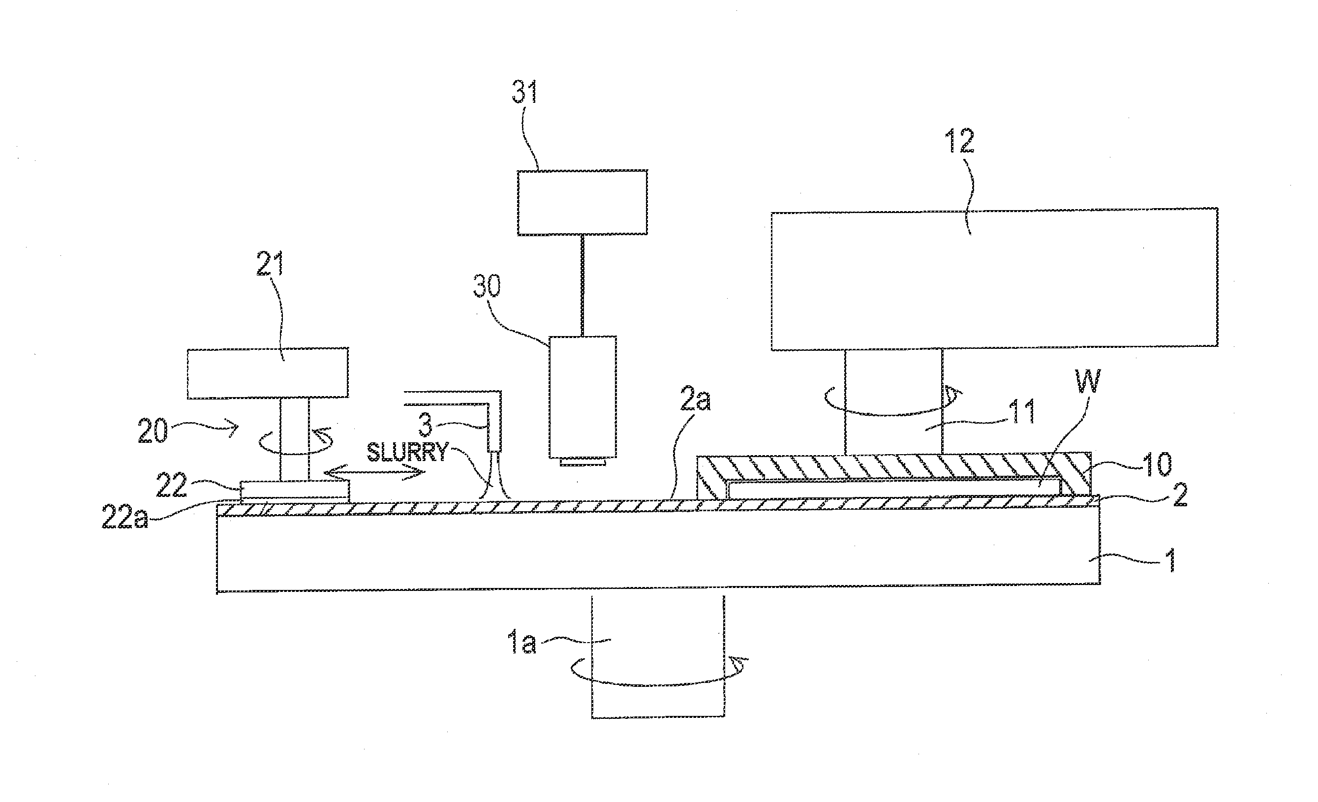
[0040]FIG. 1 is a schematic view showing an entire structure of a polishing apparatus which performs a measuring method of a surface roughness of a polishing pad according to an embodiment. As shown in FIG. 1, the polishing apparatus includes a polishing table 1, and a top ring 10 for holding a substrate W such as a semiconductor wafer as an object to be polished and pressing the substrate W against a polishing pad 2 on the polishing table 1. The polishing table 1 is coupled via a table shaft 1a to a polishing table rotating motor (not shown) disposed below the polishing table 1. Thus, the polishing table 1 is rotatable about the table shaft 1a. The polishing pad 2 is attached to an upper su...


PUM


Abstract

There is disclosed a measuring method of a surface roughness of a polishing pad which can measure a surface roughness index of the polishing pad showing a strong relationship with polishing performance. A method for measuring a surface roughness of a polishing pad includes acquiring an image of a surface of a polishing pad by using a laser microscope, selecting only a region which has a height larger than an average height from the acquired image, and calculating a surface roughness from only the selected region.

Description

CROSS REFERENCE TO RELATED APPLICATION[0001]This document claims priority to Japanese Patent Application Number 2013-172218 filed Aug. 22, 2013, the entire contents of which are hereby incorporated by reference.BACKGROUND[0002]In recent years, high integration and high density in semiconductor device demands smaller and smaller wiring patterns or interconnections and also more and more interconnection layers. Multilayer interconnections in smaller circuits result in greater steps which reflect surface irregularities on lower interconnection layers. An increase in the number of interconnection layers makes film coating performance (step coverage) poor over stepped configurations of thin films. Therefore, better multilayer interconnections need to have the improved step coverage and proper surface planarization. Further, since the depth of focus of a photolithographic optical system is smaller with miniaturization of a photolithographic process, a surface of the semiconductor device n...

Claims


Application Information

Patent Timeline
Patent Type & Authority Applications(United States)
IPC IPC(8): B24B49/12B24B53/017G01B11/30B24B37/005
CPCB24B49/12G01B11/303B24B53/017B24B37/005H01L21/304H01L22/12
Inventor MATSUO, HISANORI
Owner EBARA CORP
Why Eureka
Try Eureka