Field effect transistor, device including the transistor, and methods of forming and using same

a field effect transistor and transistor technology, applied in biochemistry apparatus and processes, instruments, material analysis, etc., can solve the problems of limited ion current blockade techniques, and limited sequencing rate to below 1000 bases per second

Active Publication Date: 2015-03-05
INANOBIO
View PDF3 Cites 9 Cited by
  • Summary
  • Abstract
  • Description
  • Claims
  • Application Information

AI Technical Summary

Benefits of technology

[0007]The present invention provides an improved field effect transistor and device that can be used to sense and characterize a variety of materials. The field effect transistor and/or device including the transistor may be used for a variety of applications, including genome sequencing, protein sequencing, biomolecular sequencing, and dete...

Problems solved by technology

While these techniques hold promise to deliver a solution that is able to read-out the three billion base pairs at low cost and in a reasonably short period of time, they suffer from few fundamental limitations.
Ion current blockade techniques are limited by relatively low ion mobility in aqueous solution, when measuring ion-current across a nanopore.
A recent study shows a current response over a time period of 104 micro seconds for a step input applied and measured across a nanopore...

Method used


Image

  • Field effect transistor, device including the transistor, and methods of forming and using same
  • Field effect transistor, device including the transistor, and methods of forming and using same
  • Field effect transistor, device including the transistor, and methods of forming and using same

Examples


Embodiment Construction

[0026]The description of exemplary embodiments of the present disclosure provided below is merely exemplary and is intended for purposes of illustration only; the following description is not intended to limit the scope of the invention disclosed herein. Moreover, recitation of multiple embodiments having stated features is not intended to exclude other embodiments having additional features or other embodiments incorporating different combinations of the stated features.

Device Structure

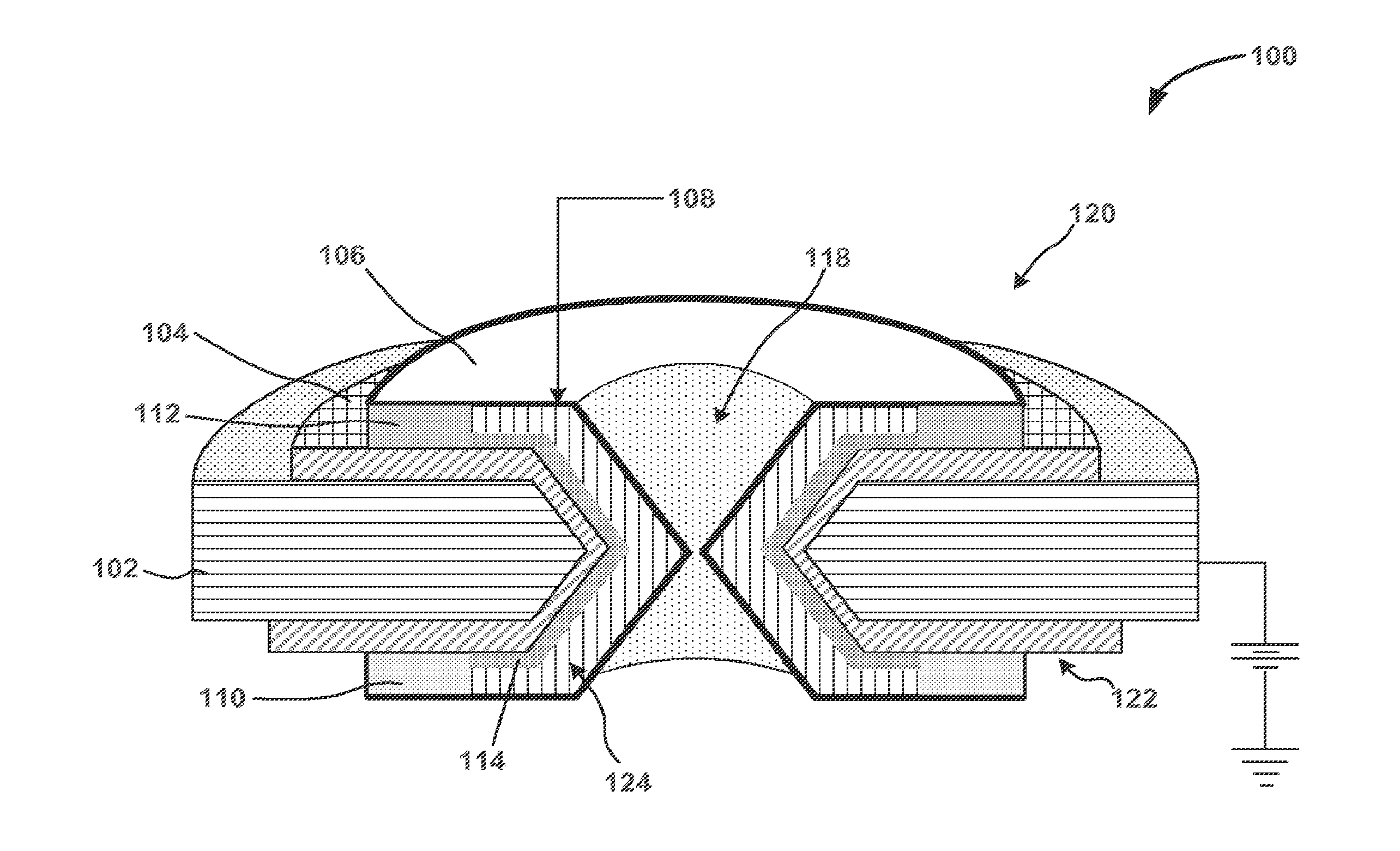
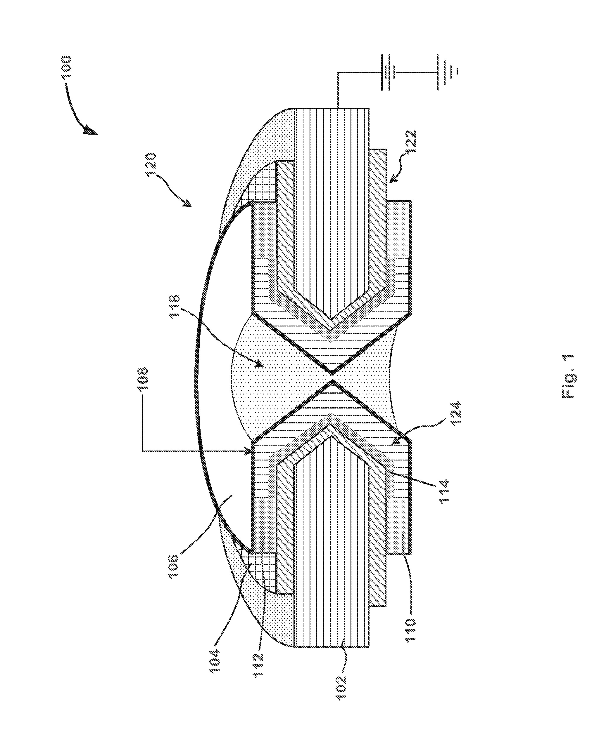
[0027]FIG. 1 illustrates a device 100 in accordance with various exemplary embodiments of the disclosure. Device 100 includes a substrate 102, an etch region 118 formed within a portion of substrate 102, an insulating region 104 formed proximate etch region 118, a source region 112 overlying insulating region 104 and a first surface 120 of substrate 102, and a drain region 110 formed overlying insulating region 104 and a second surface 122 of substrate 102. As illustrated, source region 112 and drain...


PUM

PropertyMeasurementUnit
Crystallinityaaaaaaaaaa
Metallic bondaaaaaaaaaa
Semiconductor propertiesaaaaaaaaaa

Abstract

The present disclosure provides an improved field effect transistor and device that can be used to sense and characterize a variety of materials. The field effect transistor and/or device including the transistor may be used for a variety of applications, including genome sequencing, protein sequencing, biomolecular sequencing, and detection of ions, molecules, chemicals, biomolecules, metal atoms, polymers, nanoparticles and the like.

Description

CROSS REFERENCE TO RELATED APPLICATIONS[0001]This application claims the benefit of U.S. Provisional Patent Application Ser. No. 61 / 621,966, entitled FIELD EFFECT NANOPORE DEVICE AND CHEMICAL-STOP NANOPORE ETCHING FOR GENOME SEQUENCING, PROTEIN SEQUENCING AND OTHER APPLICATIONS, and filed Apr. 9, 2012 and U.S. Provisional Patent Application Ser. No. 61 / 802,235, entitled FIELD EFFECT NANOPORE TRANSISTOR DEVICE METHODS OF FORMING AND USING THE SAME, and filed Mar. 15, 2013, the disclosures of which are incorporated herein by reference to the extent such disclosures do not conflict with the present disclosure.GOVERNMENT LICENSE RIGHTS[0002]This invention was made with government support under grant number 5R21HG006314 awarded by NIH. The United States government has certain rights in the invention.FIELD OF THE INVENTION[0003]The present invention generally relates to field effect transistors and devices including the transistors. More particularly, the invention relates to field-effect...

Claims


Application Information

Patent Timeline
IPC IPC(8): G01N27/414G01N33/543
CPCG01N27/414G01N27/4145G01N33/54366G01N33/48721C12Q1/6874G01N27/4146G01N33/54373G01N33/552H01L21/30604H01L29/0665H01L29/0692H01L29/1054H01L29/66666
Inventor TAKULAPALLI, BHARATHJAIN, ABHINAV
Owner INANOBIO
Why Eureka
Try Eureka